The spread spectrum wireless communication standard IS-95/3GPP has strict regulations on linearity and adjacent channel power ratio (ACPR). To meet the requirements, high-linearity Class A or Class AB RF power amplifiers are required in wideband code division multiple access (W-CDMA) wireless handsets. However, at an output power of +28 dBm, the power added efficiency (PAE) of this type of power amplifier is only about 35% at most; if the output power is reduced, the PAE value is lower.
The power amplifier does not continue to operate in talk mode. When the mobile phone user does not speak, the power amplifier will operate at half rate (50% working time) or 1/8 rate, so there is no need to worry about the phone heating when in the call mode. However, in data mode, the power amplifier will work until the data transfer is complete. The low efficiency and continuous operation of the power amplifier quickly drains the battery, and the resulting internal power consumption can overheat the handset.
Power consumption is a major challenge for early W-CDMA handsets that support high-speed data transmission services. It forces designers to use larger heat sinks, stronger cooling airflow, and larger capacity batteries. Fortunately, these problems have been alleviated over the past few years as power amplifiers for CDMA and W-CDMA handsets have made significant advances in power efficiency.
In CDMA and W-CDMA systems, the RF power output of the power amplifier is not always the largest. In order to optimize the cellular capacity (the number of transmission channels that the base station can handle simultaneously), each handset must control its RF output power so that the effective signal-to-noise ratio received by the base station is identical.
From the probability distribution of the RF output power of many mobile phones in a specific area, the average output power of a standard CDMA or W-CDMA mobile phone is: about +10 dBm in the suburb; about +5 dBm in the city. Therefore, an effective goal to improve the efficiency of the power amplifier is not the maximum power level, but to find a suitable range between +5dBm and +10dBm.
Two supply voltages are required for CDMA and W-CDMA power amplifiers (see figure). VREF provides bias for the internal driver stage and power amplifier stage, while VCC is used to bias the collector of the driver and power amplifier. By adjusting these two voltages, the designer can reduce the supply current of the power amplifier.
When the RF transmit power is zero, the power amplifier automatically pulls the quiescent current to 100mA (typ), while VREF and VCC are 3V and 3.4V, respectively. Reducing VREF from 3V to 2.9V reduces the quiescent current by approximately 20mA.
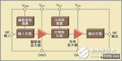
F1: Two supply voltages are required in the CDMA/W-CDMA handset power amplifier design : Vref and Vcc. The operating current of the power amplifier can be reduced by adjusting these two voltages. Therefore, the designer can reduce the quiescent current of the power amplifier to a large extent by lowering the VREF, but to ensure that the linearity and ACPR of the power amplifier are not lower than the specification.
Lower VREF and VCCIf we have an empirical value that provides the minimum VREF voltage required for the different output power levels of the power amplifier, then the VREF control can be actively combined with the power control process of the amplifier. If this method is too difficult, we can simply perform two-stage regulation of VREF, corresponding to low power mode (less than 10dBm) and high power mode (greater than 10dBm).
In order to adjust VREF through the fundamental frequency control D/A converter, we chose a low power operational amplifier with large output current capability and external gain adjustment. In a typical wireless handset, the VCC of the power amplifier is taken directly from a single-cell Li-ion battery, so the VCC operates from 3.2V to 4.2V. As noted above, statistical data indicates that power amplifiers for CDMA and W-CDMA operate at power levels of +5 to +10 dBm most of the time.
At this level, designers can significantly reduce VCC without losing power amplifier linearity while reducing power consumption due to excessive collector bias. Experimental tests at low power levels have shown that while the collector bias continues to be below 0.6V, we can still maintain normal communication with the base station. A variable bias voltage is provided to the power amplifier collector through a specially designed high efficiency dc/dc buck converter. We can use a dedicated digital analog converter output of the baseband processor to adjust the output voltage of the buck converter. The dc/dc converter that controls the collector voltage of the power amplifier must be able to respond quickly to the control signal. Typically, the output voltage of the dc /dc converter should be within 90% of the new set voltage within 30 microseconds after the analog control level change from the baseband processor. The converter die provides an appropriate internal gain between its VCC control input and the output voltage that biases the collector of the power amplifier. It also performs switching at high frequencies to reduce the size of the inductor.
Connecting a dc/dc converter between a power amplifier and a battery can exacerbate the problem of requiring high RF power at low battery voltages. To provide +28dBm of RF power while maintaining the linearity of the power amplifier, manufacturers recommend a minimum VCC of 3.4V. In order to maintain 35% PAE at 3.4V, we also need a power amplifier collector current of up to 530mA.
+28dBm RF power: 102.8 mW = 631mWRequired power amplifier power (VCC ICC): 631mW / (PAE / 100) ~ 1,803mW. The required power amplifier current (ICC) at VCC = 3.4V: ICC = 1,803mW/3.4V = 530mA. To support 3.4V VCC and 530mA ICC, the dc/dc converter acting as a power amplifier supply requires a certain input-output margin. For example, if the converter's internal P-channel MOSFET (PFET) has an on-resistance of 0.4Ω and the inductor impedance is 0.1Ω, then the series drop across the two components is (0.4Ω+0.1Ω) 530mA = 265mV. Therefore, when the battery voltage is lower than 3.665V, the dc/dc converter cannot support the 3.4V output.
In the case where the battery voltage is lower than 3.665 V, it is preferable to short the power amplifier collector to the battery. Otherwise, you will not be able to fully utilize the power of the lithium-ion battery. The usual solution is to bypass the inductor and the internal PFET by paralleling a low Rds PFET. This bypass FRET (built-in or external) connects the battery voltage directly to the collector of the power amplifier in high power mode. In order to satisfy both high RF power and low battery voltage, this bypass method must be employed.
Optimize PAEThe best practice for optimizing PAE is to continuously adjust the bias voltage of the collector of the power amplifier. However, this approach requires factory calibration and complex software to ensure good PA linearity and ACPR with continuous collector bias voltage variations. The second best practice is to step-adjust the collector bias voltage, usually two to four orders.
For example, in a fourth-order system, the VCC values ​​included may be: Vbatt, 1.5V, 1V, and 0.6V. The overall efficiency of the system is comparable to that of a system that continuously controls the power amplifier's collector bias, and at low or medium power levels, the inductor only needs to provide a peak current of less than 150mA.
Insulated Copper Tube Terminals
Insulated Copper Tube Terminals,High quality insulated terminal,copper tube terminal
Taixing Longyi Terminals Co.,Ltd. , https://www.longyicopperterminals.com