Before using serdes has been running relatively low-speed applications, 3.125Gbps, according to the official documentation step by step has not had any problems, this time I want to verify the K7 series GTX maximum line speed 8Gbps, look at the xilinx FPGA is not like According to the official document.
How much can GTX speed run?On the issue of device speed, first find ds182->Kintex-7 FPGAs Data Sheet: DC and AC Switching CharacterisTIcs, you can find the corresponding device, but this should be considered when designing the device selection, unless it is bought The development department uses it. This includes the highest frequency and device delay that all FPGA devices can reach, setup time, hold time, etc., which has great reference value for high-speed design.
Find GTX Transceiver Switching CharacterisTIcs
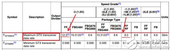
It can be seen that although the K7 series GTX can run up to 12.5Gbps, it has a relationship with the speed grade and the package. It is at the speed level of -3, and the maximum speed of 12.5Gbps is only available under the FF package. Now the chip model at hand is K7480TFFG901-1, so it supports up to 8.0Gbps. In fact, this will be found when configuring the IP core, the line speed range is (0.5-8.0). So the IP core is strictly related to the engineering device, and Vivado is getting better and better.
Step by step configuration of the IP coreThe following steps to configure the IP core can be used as a reference for beginners. (If you use it for the first time, it will be a lot of files generated and a lot of IO ports scared.) How to find the manual and schematic, go through the process and find that the IP core of xilinx is a routine.
1. First search the GT in the IP core and select the 7 Series FPGAs TransceiversWizard.
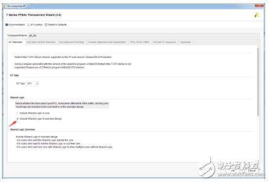
No choice, take a name. Incidentally, the following shared logic options, preferably include shared logic in example design. I have encountered problems here when some special resources need to be shared. Of course, it is not a GTX module. It is a module of Ethernet RGMII. IDELAY should use IODELAY_CTRL, and an IOB will be used. When the same IOB is used elsewhere, you must select the following option. So it is best to choose the next one, no problem.
2. Next is more important
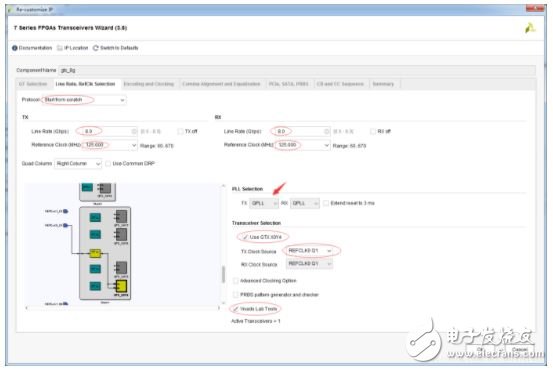
The first is the agreement, the simplest strat from cratch, there is no agreement. Then there is the line speed, and the range is (0.5-8.0). The reference clock, this can be selected as needed. The software calculates the options for the reference clock based on your line speed. The receiver is also set up, of course, can be different. This is full-duplex, the transceiver link has nothing to do, you can also turn off one of Tx off or Rx off. Then there is the PLL selection. Which one to choose? Let's go back to the ds182 we just mentioned, the same part of the table.
In fact, the line speed has decided that it has not been chosen, it has become gray.
Then it is more important, choose which transceiver to use, which of course is not decided by the head, related to the design, you can find the schematic.
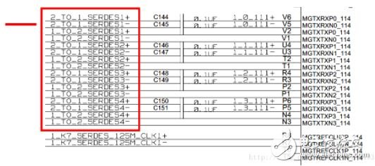
For example, check the manual UG476-> 7 Series FPGAsGTX/GTH Transceivers to find the Placement InformaTIon by Package as follows
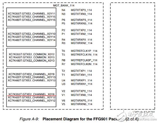
This will know that X0Y8 is used, and the input clock can be found in the above schematic, which is the same group of clk0.
Finally, check the vivado lab tools so that you can produce the example project for reference.
3. Continue
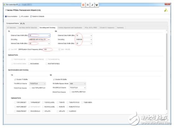
I have been using 8b10b before, this time try 64b66b, which is originally an encoding protocol under high bandwidth, which is more efficient. Why use 8b10b, 64b66b including the following scrambling code in one sentence is to increase the frequency component is beneficial to CDR (clock data recovery) and reduce DC, the two are different reasons. Specific can be Baidu. The bottom optional port is removed for simplicity.
4.
Since there is no choice of 8b10b, this page is not optional, and all the optional ports below are still removed.
5.
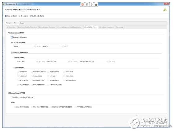
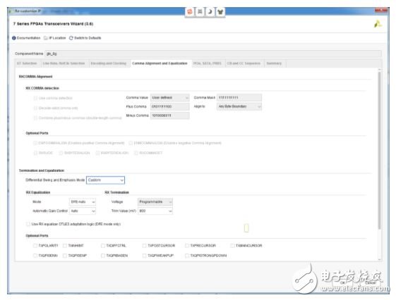
Ok, pcie keeps the next study, it's too complicated. The optional port is actually quite useful, adding controllability, such as loopback control, LOOPBACK. By the way, there are four internal loopbacks.
1. "000": normal mode does not loop back
2. "001": Near-end PCS loopback
3. "010": Near-end PMA loopback
4. "100": Remote PMA loopback
5. "110": remote PCS loopback)
6. Next is channel bonding and clock correction
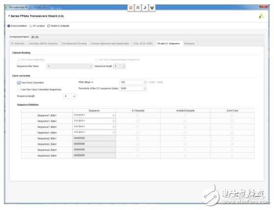
The function of channel binding is to align multiple physical channels and bind them into one logical channel. In fact, the FIFO is used to eliminate the delay uncertainty between channels. Since there is only one channel, there is no binding at all.
7. Finally, look at the confirmation right, pay attention to the transceiver clock is 250M. Can count, 8000M/32=250M.

I have completed more than half of it here.
Generate an example project using an IP core
Next generate the example project
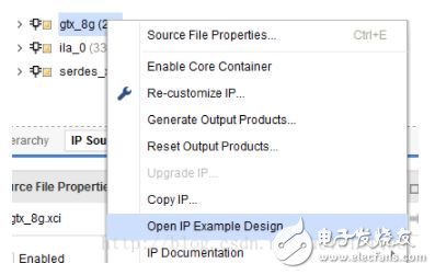
Right-click the IP just configured, as shown in the figure.
After the generation, slightly change the constraint file XDC and constrain the input clock of the DRC clock. Nothing else.
## LOC constrain for DRP_CLK_P/N
Set_property LOC G27 [get_ports DRP_CLK_IN_P]
Set_property LOC F27 [get_ports DRP_CLK_IN_N]
Set_property IOSTANDARD LVDS_25 [get_ports DRP_CLK_IN_P]
Set_property IOSTANDARD LVDS_25 [get_ports DRP_CLK_IN_N]
It can be found which transceiver can be used directly here. Note: The effect changed here is the same as the one set in step 2 above.
Set_property LOC GTXE2_CHANNEL_X0Y4 [get_cells gtx_8g_support_i/gtx_8g_init_i/inst/gtx_8g_i/gt0_gtx_8g_i/gtxe2_i]
If you want to change it, of course, the clock of GTX has to be changed.
Set_property LOC AD5 [get_ports Q1_CLK0_GTREFCLK_PAD_N_IN ]
Set_property LOC AD6 [get_ports Q1_CLK0_GTREFCLK_PAD_P_IN ]
Then modify a place, the original ILA core is the data before the descrambling code, and the data after the descrambling code can be replaced to see the received data more clearly.
Board debugging verification
Well, the generated bit goes in, you can use the connection line to connect with a single send of a serdes, or set the internal loopback, or experiment on two FPGAs.
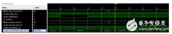
It can be seen that error_count is always 0, indicating that the transceiver is correct and stable.
The received data is 00000fb, 3020100, 7060504... in order, and the sending file is opened as follows, and the same is sent.
00000000000000fb0100
00000000030201000000
00000000070605040000
000000000b0a09080000
The experiment proved that GTX can run up to 8.0Gbps.
The generated example project can be studied and studied. There are scrambling codes and descrambling codes. You can modify the data after descrambling to compare them. You can clearly see what data was received. Including how the verification module is verified, it is worth learning.
We've been around for over 16+ years. We make sure our sound is The Best Sound.
Our products include gaming headset, Bluetooth Earphone, Headphones Noise Cancelling, Best Wireless Earbuds, Bluetooth Mask, Headphones For Sleeping, Headphones in Headband, Bluetooth Beanie Hat, bluetooth for motorcycle helmet, etc
Manufacturing high-quality products for customers according to international standards, such as CE ROHS FCC REACH UL SGS BQB etc.
We help 200+ customers create custom Bluetooth headphones, earbuds, earphones, etc audio products design for various industries.
Customized Headphones, personalized gifts, promotional products custom , Bluetooth Earphones,Best Headphones
TOPNOTCH INTERNATIONAL GROUP LIMITED , https://www.mic11.com