Low Noise Amplifier (LNA) is widely used in the fields of radio astronomy, satellite receiving, radar communication and other receivers with high sensitivity requirements. The main function is to amplify the received weak signal, reduce noise, and demodulate the system. The required information data. The Noise Figure (NF) as an important technical indicator directly reflects the sensitivity of the entire system, so the LNA design is critical to the performance of the entire system.
1 GPS receiver low noise amplifier designThe main indicators of the designed LNA are: operating frequency is 1 520 ~ 1 600 MHz; noise figure NF16.0 dB; input standing wave ratio "2; output standing wave ratio "1.5.
1.1 Device Selection
Choosing the right device, considering the lower noise figure and higher gain, choose PHEMT GaAsFET low noise transistor. Before designing a low-noise amplifier, first establish a small-signal model of the transistor, and the average company will provide an amplifier with a ready-made model. Here, Agilent's ATF-54143 is selected. In the 1.52 to 1.60 GHz band, a reverse-Ï„ type matching network is designed, which is composed of lumped element inductance and capacitance. When selecting an inductor, choose a high Q inductor. In order to be able to match the actual situation in the simulation, the inductance and capacitance model of Murata is used. Here, the chip inductor type is LQWl8, the chip capacitor model is GRMl8, and the inductor LQWl8 has a typical Q value of 80 at 1.6 GHz.
1.2 DC offset
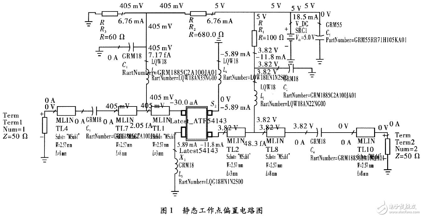
In designing a low noise amplifier, the goal of designing a DC bias is to select a suitable static operating point. The quality of the static point directly affects the noise, gain, and linearity of the circuit. A simple bias network consisting of resistors provides the ATF-54143 with a suitable static operating point, but with poor temperature. Active bias networks can be used to compensate for the shortcomings of temperature, but active bias networks can increase circuit size, increase board layout and increase power consumption. In designing the actual circuit, the active bias network or the resistor bias network should be selected according to the specific situation. For the LNA in this paper, the resistor passive bias network is chosen here considering the structure and cost. Agilentl's ATF54143 was used to design a Vds=3.8 V, Ids=ll mA bias operating point based on the datasheet specifications given by the company. Because ATF-54143 performs better when the current is llmA. Resistor R3 is 100 Ω; R2 is 680 Ω; R1 is 60 Ω, as shown in Figure 1.
1.3 Stability design
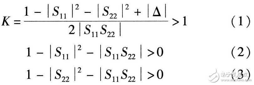
The stability of the amplifier is an important factor to consider in the amplifier. Need to be absolutely stable at the operating frequency, there are two ways to judge the device is unconditionally stable. the first method
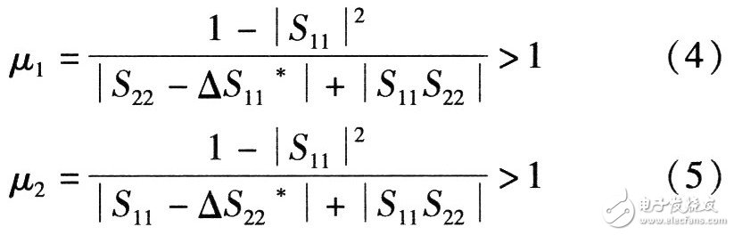
The second method: using the s parameter combination test standard, only a single parameter μ, which is defined as
There are two ways to stabilize the circuit: the first is to add a resistive load to the drain of the FET to enable the device to generate equal impedance over a wide frequency band for broadband stability. The disadvantage is that the resistive terminal consumes some energy and reduces the output power. Secondly, adding an inductance between the source and the ground can cause series negative feedback, which reduces the gain of the device, but the stability is improved. In the microwave circuit, the source negative feedback can be an inductor lumped component or a short transmission line. The former uses the former design.
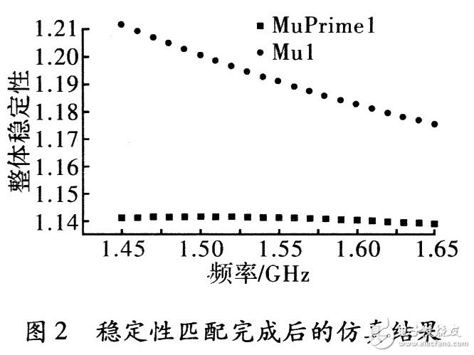
The simulation results are shown in Fig. 2 and Fig. 3. It can be seen that the input and output and the overall stability are all in the range of l 520 to l 600 MHz, so the circuit is stable in the band.

1.4 Input and output impedance matching circuit design
When designing the LNA, the input matching cannot use the conjugate matching method, but the best source reflection coefficient noise matching. The input impedance matching network circuit consists of C4 and L5. As shown in Figure 3, the network can effectively reduce the return loss and improve the gain and stability within the band. L1 acts as a DC and 扼 AC, and C1 acts as a RF bypass. The Q values ​​of inductors L1 and L5 play an important role in reducing circuit losses and reducing NF(2) at the input. A low inductance Q value increases the input noise, which affects the total noise of the entire circuit.
The output matching uses a conjugate matching design. The output impedance matching network consists of C6 and L7, as shown in Figure 4, reducing return loss and increasing gain. C2 acts as a radio frequency bypass and C5 acts as a power supply decoupling.
Use the Smith software to simply find the value of the matching network lumped component and then optimize it with ADS software. When optimizing, pay attention to the following points: Firstly, adjust the parameters of each device manually by tuning function, know which device parameters have great influence on the circuit index, and handle the sensitive device parameters carefully; secondly, set the optimization target; finally, when optimizing, Avoid self-oscillation.
1.5 LNA circuit overall optimization
After the DC bias design, stability design and matching network design, the LNA structure is basically fixed, but in order to meet the requirements of various indicators, it is also necessary to optimize the values ​​of each device, and also consider the actual circuit microstrip line, short circuit grounding, via The impact, so the overall simulation of the circuit needs to be optimized.
Usually in the RF circuit, the microstrip line is used to transmit signals. It is necessary to pay attention to the width of the microstrip line, and the width determines the characteristic impedance. A 50 Ω characteristic impedance is typically used for the input and output ports. In this design, the plate was selected to have a constant constant of 2.65 and a thickness of 1 mm. Using Agilent's Appcad software, the width of the microstrip line can be calculated to be 2.57 mm.
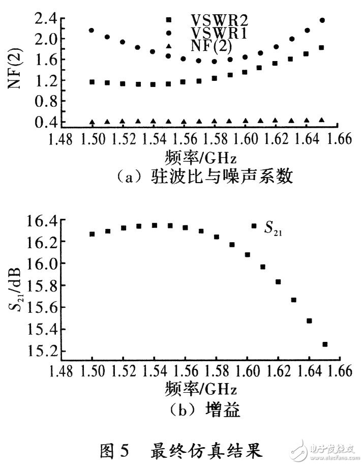
When optimizing the LNA circuit, the setting of the optimization index should be reasonable. In the process of optimizing the indicators, it is necessary to make full use of the tuning function, first know the approximate value of the parameters, and then optimize the parameters on this basis until the desired effect is achieved. The final simulation results are shown in Figure 5.
Copper Tube Terminals Without Checking Hole
Our company specializes in the production and sales of all kinds of terminals, copper terminals, nose wire ears, cold pressed terminals, copper joints, but also according to customer requirements for customization and production, our raw materials are produced and sold by ourselves, we have their own raw materials processing plant, high purity T2 copper, quality and quantity, come to me to order it!
Copper Tube Terminals Without Checking Hole,Cable Lugs Insulating Crimp Terminal,Cable Connector Tinned Copper Ring Terminal,Tubular Cable Lugs Crimp Terminal
Taixing Longyi Terminals Co.,Ltd. , https://www.longyicopperlugs.com