Abstract: For the LTE-A mobile terminal application, a broadband power amplifier is designed with dual power mode architecture, which improves the efficiency of the power amplifier's retracted area by switching the working mode of the power amplifier. The power amplifier also adopts an integrated process of InGaP/GaAs HBT and AlGaAs/InGaAs pHEMT, which integrates the power amplifier circuit and the control circuit monolithically to realize on-chip switching of mode control, which can effectively improve the integration degree of the power amplifier. The power is placed at a working voltage of 3.4 V and a frequency of 2.3 to 2.69 GHz. Using a 10 MHz LTE modulated signal input, the LPM is improved by at least 6% relative to the HPM at an output power of 10 dBm, effectively increasing the power of the amplifier. The efficiency of the fallback, the performance of the amplifier meets the 3GPP protocol requirements in the full frequency band.
Keywords: dual power mode; power backoff; efficiency improvement; power amplifier
CLC number: TN927
Document identification code: A
DOI: 10.16157/j.issn.0258-7998.171431
Chinese citation format: Huang Liang, Li Jiajin, Zhang Guohao. A dual power mode wideband power amplifier design for LTE-A[J].Application of Electronic Technique, 2017, 43(9): 30-33, 38.
English reference format: Huang Liang, Li Jiajin, Zhang Guohao. A dual power mode broadband power amplifier design for LTE-A applications [J]. Application of Electronic Technique, 2017, 43 (9): 30-33, 38.
0 Preface
In wireless communication systems, Power Amplifiers (PAs) are one of the important factors affecting the endurance of handheld mobile terminals. In particular, LTE-A mobile communication networks place higher demands on the linearity and efficiency of power amplifiers. LTE-A is an abbreviation of LTE-Advanced and is an evolution of LTE. The LTE-A protocol uses Orthogonal Frequency Division Multiplexing (OFDM) technology, which has high spectral efficiency and large peak-to-average power (PAPR). For example, if the LTE-A QPSK modulated signal has a bandwidth of 10 MHz and the number of Resource Blocks is 12 RB, the PAPR of the signal can reach more than 7 dB [1]. Due to the high PAPR of the LTE-A system signal, the power amplifier mainly works in the power back-off area away from the highest linear output power, resulting in a decrease in the average efficiency of the power amplifier, which greatly reduces the use time of the mobile terminal.
At present, there have been many studies on the average efficiency improvement technology of power amplifiers. Representative technologies such as Envelope Elimination and Recovery (EER) [2] and Envelope Tracking (ET) [3] both adjust the supply voltage of different input signals according to the signal envelope through an additional supply voltage modulation module. In order to increase the average efficiency of the power amplifier; however, its additional control circuit increases the size of the chip, increasing the complexity and cost of the power amplifier.
Therefore, this paper describes a power amplifier with two power modes, High Power Mode (HPM) and Low Power Mode (LPM), to improve the efficiency of the power amplifier in the low power output region. The two power modes are respectively designed with corresponding linear power amplifiers, and mode switching is achieved by switching. The switch is designed using a simple and practical pHEMT process, and the switching process can be implemented on the same wafer as the InGaP/GaAs HBT process. Therefore, the application of these two processes can realize the dual-power mode power amplifier single chip, reducing the size of the power amplifier. In addition, in order to simplify the RF front end, a broadband design will also be adopted.
1 Design and analysis of power amplifier
Based on the above design considerations, a schematic diagram of a dual-power mode wideband power amplifier operating at 2.3 to 2.69 GHz with a supply voltage of 3.4 V is shown in Figure 1. Figure 1 shows the schematic diagram of the power amplifier. The shaded part is the single-chip integrated (MMIC) part. Only the output matching and power supply are realized through off-chip. The control circuit and the bias circuit are also integrated on the same die as the power amplifier.

In the power amplifier architecture shown in Figure 1, the HPM link consists of SW1, Q1, Q2, and Q3; the LPM link consists of SW2, SW3, Q4, and Q5. In the high power mode, the power amplifier stages Q1, Q2, and Q3 operate, the power amplifier stages Q4 and Q5 are turned off, the RF switch SW1 is turned on, and the RF switches SW2 and SW3 are turned off. In the low power mode, the power amplifier stages Q1, Q2, and Q3 are turned off, the power amplifier stages Q4 and Q5 are working, the RF switch SW1 is turned off, and the RF switches SW2 and SW3 are turned on. The on and off of the amplifier and switch are controlled by bias and switch control circuits, respectively.
1.1 High and low power amplifier design
The HPM link of the amplifier is implemented by a three-stage power amplifier, as shown in Figure 1. The first stage of the power amplifier should provide sufficient driving for the rear stage. The first stage is biased in class A to improve the linearity of the whole power amplifier and provide high gain. Since the first stage output power is small, the emitter area is small. The size of the power amplifier is 300 μm2; the second stage of the power amplifier is the power amplifier driver stage, which mainly enables the output stage to obtain sufficient power output. The output stage is biased to the shallow class AB, and the drive output has an emitter area of ​​840 μm2; the third stage is mainly The function of power amplification is biased in the deep AB type to improve the efficiency of the power amplifier. Due to the large operating current, the emitter area is 4 500 μm 2 . In order to achieve broadband, the RC negative feedback network is applied to both the first stage and the second stage of the power amplifier. The negative feedback network can increase the gain flatness of the power amplifier and reduce the nonlinear influence of the power amplifier tube to some extent. In addition, a two-stage LC broadband efficient matching structure is adopted between the second and third levels.
The LPM link of the amplifier is implemented by a secondary power amplifier, as shown in Figure 1. The first stage of the power amplifier needs to provide gain and provide sufficient driving for the rear stage. The first stage is biased in class AB and the emitter area is 300 μm2. The second stage mainly functions as power amplification, and its bias is In the deep AB class to improve the efficiency of the power amplifier, its emitter area is 540 μm2. In order to increase the bandwidth, the first stage of the amplifier uses an RC negative feedback network.
The HPM output matching network of the power amplifier adopts a two-stage LC series matching network to improve the bandwidth of the output matching network. In addition, in order to obtain higher harmonic suppression in a wider frequency range, improve the efficiency and linearity of the power amplifier, the power amplifier output The collector adds two parallel harmonic suppression networks. The goal of the LPM is to operate in the linear back-off zone of the power amplifier, such as a power backoff of 10 dB. The two modes set the optimal impedance separately, so the power amplifier efficiency can be improved when the power is backed up.
1.2 Control circuit design
The control circuit shown in FIG. 1 includes a voltage reference circuit, a logic control circuit, and a power amplifier bias voltage control circuit.
The voltage reference circuit is shown in Figure 2, through which the bias voltage Vreg can be supplied to the bias circuit of the power amplifier. The reference circuit is a simple mirror circuit, and the reference voltage Vreg is provided to the bias circuit through the transistors Q6, Q7 and the resistor R; the circuit can control the operation and the shutdown of the reference circuit by the high and low potentials of the enable terminal Ven; When the reference circuit is turned off, it means that the entire amplifier is turned off.

Figure 3 shows the power amplifier mode switching circuit, including the logic control circuit and the power amplifier bias voltage control circuit. Figure 3 (a) is a logic control circuit, through which the power mode of the power amplifier can be switched; when Vmode is connected to a low level, the HPM point is high level, the LPM point is low level, the power amplifier is turned on the high power mode channel; At the level, the HPM point is low and the LPM point is high, and the amplifier turns on the low power mode channel. Figure 3 (b) is the power amplifier bias voltage control circuit, through which the power amplifier bias circuit can be controlled to open and close; when in high power mode, Vreg = VBias_HPM, VBias_LPM is low, high power link bias open The low power circuit is biased off; when in low power mode, Vreg = VBias_LPM, VBias_HPM is low, the high power link bias is off, and the low power circuit is biased open.

2 power amplifier implementation
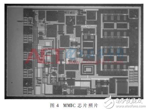
The dual-power mode wideband power amplifier designed in this paper was successfully taped using Win Semiconductors' InGaP/GaAs HBT and AlGaAs/InGaAs (D-Mode) pHEMT processes. As shown in FIG. 4, the MMIC chip photograph after the flow sheet has a size of 750 μm×950 μm. After the chip is bonded to the substrate, the final fabricated power amplifier chip has a size of 3 mm × 3 mm.
The MMIC power amplifier designed in this paper, as shown in the shaded part of Figure 1, only the output matching and power supply are realized through off-chip, and the control circuit and bias circuit are also integrated with the power amplifier on the same chip die. Due to the high integration of the power amplifier designed in this paper, the RF path and the DC path are laid out separately in the layout of the layout, and the HPM, LPM and control circuit of the power amplifier are arranged in a sub-area; the RF and DC paths are laid out separately, which can effectively ensure the performance of the power amplifier.
3 power amplifier test results and analysis
In order to test the performance of the chip, the chip will be mounted on the PCB test board of the FR_4 board for performance testing. The power amplifier operates at 3.4 V. The small-signal S-parameters S11 and S21 of the power amplifiers HPM and LPM are measured using Agilent's network analyzer E5071C. At HPM, the quiescent current is 87 mA, with quiescent currents of 15 mA, 26 mA, and 48 mA from the first to the third, and S21 over the range of 2.3 to 2.69 GHz; the parameter S11 is at the frequency. It is also less than -10 dB between 2.3 and 2.69 GHz. At LPM, the quiescent current is 20 mA, with quiescent currents of 8 mA and 12 mA from the first and second stages, respectively; S21 exceeds 17 dB in the 2.3 to 2.69 GHz band, and S21 is highest at 2.5 GHz. The value is 20 dB; the parameter S11 is also below -8 dB at frequencies between 2.3 and 2.69 GHz. The above shows that the small signal parameters are good, and the wide frequency band of the small signal is realized in the high power mode.

Use Agilent's signal generator N5182A and signal analyzer N9030A to build a large signal test platform; set the power supply voltage of the power amplifier to 3.4 V, and modulate the signal source to LTE-FDD-10M-12RB, the signal frequency is 2.3 GHz, 2.5 respectively. The gain (Gain), output power (Pout), power added efficiency (PAE), E-UTRAACLR1 and UTRAACLR1 of the power amplifier at frequencies of 2.3 GHz, 2.5 GHz and 2.69 GHz are measured at GHz and 2.69 GHz, respectively. Figure 6, Figure 7, Figure 8, and Figure 9. Both E-UTRAACLR1 and UTRAACLR1 are the ratio of the signal power in the band to the power leaked into other bands due to non-linearity. They represent whether the PA interferes with the input signal and the interference to other frequency bands is serious. Among them, E-UTRAACLR1 represents 4G to 4G (ie LTE to LTE) interference, and UTRAACLR1 represents 4G interference to 3G (such as LTE to WCDMA). .

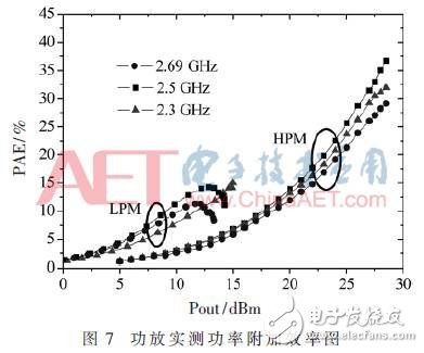
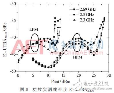

Figure 6 is an AM-AM diagram of the power amplifier operating at HPM and LPM. As can be seen from the figure, in HPM, the gain (Gain) reaches 28.5 dB in the frequency band, which satisfies the 4G system index. It can also be seen from the figure that the power output P1dB of HPM has exceeded 28 dBm, achieving high linearity of the power amplifier. , meets the maximum output power requirement of LTE_A, which indicates that the output matching state is good. In LPM, the in-band gain (Gain) fluctuates between 16.5 and 20 dB, but decreases by nearly 1 dB compared to the simulation result. It can also be seen from the figure that the LPM power output P1dB has exceeded 12.5 dBm, reaching the target. Set the maximum linear output requirement of at least 11 dBm.
Figure 7 is a power added efficiency (PAE) plot of the power amplifier operating at HPM and LPM. As can be seen from the figure, in HPM, the highest efficiency of the power amplifier is up to 30% in the frequency band, and the optimum efficiency at 2.5 GHz is 38%; in LPM, the highest efficiency of the power amplifier reaches 12 in the frequency band. %; where the output power is 10 dBm, the LPM is improved by at least 6% relative to the HPM efficiency; thus, it can be seen that the dual power mode power amplifier can effectively improve the efficiency of the power amplifier in the power back-off region.
Figure 8 is a graph showing the linearity (E-UTRAACLR1) of the power amplifier operating at HPM and LPM. As can be seen from the figure, in the HPM, when the output is 28 dBm, the in-band linearity E-UTRAACLR1 is lower than -35 dBc. It can be seen that the linear index E-UTRAACLR1 of the 4G system must be less than -30 dBc when it is HPM. In LPM, when the output is 12.5 dBm, the in-band linearity E-UTRAACLR1 is all lower than -35 dBc. It can be seen that the power amplifier can be switched to LPM when the power falls back below 12.5 dBm.
Figure 9 is a linearity (UTRAACLR1) diagram of the power amplifier operating at HPM and LPM. As can be seen from the figure, in the HPM, when the output is 28 dBm, the in-band linearity UTRAACLR1 is all lower than -36 dBc. It can be seen that the linearity indicator UTRAACLR1 that satisfies the 4G system at HPM must be less than -33 dBc. At LPM, the in-band linearity UTRAACLR1 is all below -36 dBc at 12.5 dBm output.
Table 1 compares the main performance of HPM and power amplifier research and products of the power amplifier designed in this paper. From the comparison of the table, it can be seen that the power of this chapter is designed to achieve broadband, while the power amplifier also obtains higher linearity and efficiency. In addition, compared with the products of Avago Technologies, a major international manufacturer in the literature [6], the performance of the power amplifier designed in this chapter has reached the product level, but it has a slightly lower efficiency than the single-band application amplifier, and has obvious practical value.

4 Conclusion
Based on InGaP/GaAs HBT and AlGaAs/InGaAs (D-Mode) pHEMT process, a wideband power amplifier for LTE-A is designed. The package chip size is 3 mm × 3 mm, and the power of the amplifier is improved by using dual power mode. The efficiency of the area. The chip test results show that the chip satisfies the application of Band 38, Band 40, Band 41 and Band 7 of 4G mobile communication system band simultaneously; the dual power mode of the power amplifier can effectively improve the efficiency of power amplifier in the power retreat area; The implemented RF power amplifier has a simple structure and high integration, which can effectively simplify the RF front-end application.
references
[1] HAU G, HUSSAIN A, et al. A 3×3mm2 LTE/WCDMA dual-mode power amplifier module with integrated high directivity coupler [C]. IEEE Bipolar/BiCMOS Circuits and Technology Meeting.Atlanta: IEEE Press, 2011: 138-141.
[2] VASIC M, et al. Efficient and linear power amplifier based on envelope elimination and restoration [J]. IEEE Transactions on Power Electronics, Jan 2012, 27(1): 5-9.
[3] SANGSU J, KYUNGHOON M, et al. CMOS saturated power amplifier with dynamic auxiliary circuits for optimized envelope tracking [J]. Microwave Theory and Techniques, IEEE Transactions on. 2014, 62(12): 3425-3435.
[4] KANG D, KIM D, CHO Y, et al. Design of bandwidth-enhanced doherty power amplifiers for handset applications [J]. IEEE Transactions on Microwave Theory & Techniques, 2011, 59(12): 3474-3483.
[5] HASSAN M, LARSON LE, LEUNG VW, et al. A wide-band CMOS/GaAs HBT envelope tracking power amplifier for 4G LTE mobile terminal applications[J]. IEEE Transactions on Microwave Theory and Techniques, 2012, 60 (5 ): 1321-1330.
[6] Avago Technologies.ACPM-5007 Datasheet[EB].
Floor Display,Floor-Standing Lcd Display,Floor Standing Pop Up Display,Floor Advertising Screen Display
Kindwin Technology (H.K.) Limited , https://www.szktlled.com