The LTC6802 is a battery monitoring chip that includes a 12-bit resolution analog-to-digital converter, a precision voltage reference source, a high voltage input multiplexer and a serial interface. Each LTC6802 can measure 12 series battery voltages with a maximum allowable measurement voltage of 60 volts. All battery voltages can be monitored simultaneously or any of the series batteries can be monitored separately. The chip uses a unique level-shifting serial interface. Multiple LTC6802s can be connected in series without the need for optocouplers or isolation devices between the chips.
Multiple LTC6802s can work simultaneously in series, and the voltage measurement time of all series batteries is within 13ms. To reduce power consumption, the LTC6802 also provides real-time monitoring of the overvoltage and undervoltage conditions of each cell. A MOS switch is connected to each of the battery input terminals for discharging the overcharged battery.
LTC6802 pin diagram and pin function: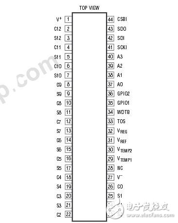
V+: Connect the positive pole of the power supply. V+ must be at the same potential as C12.
C12, C11, C10, C9, C8, C7, C6, C5, C4, C3, C2, C1 (Pins2, 4, 6, 8, 10, 12, 14, 16, 18, 20, 22, 24):
C1~C12 are voltage monitoring input pins, which can monitor up to 12 batteries. C1 is connected to V-, C2 is connected to C1, and so on.
S12, S11, S10, S9, S8, S7, S6, S5, S4, S3, S2, S1 (Pins3, 5, 7, 9, 11, 13, 15, 17, 19, 21, 23, 25)
S1 - S12 and used for battery balancing. If a section of the series battery is overcharged, the S pin can be used to discharge it.
V-: Connect the battery negative
NC: Internally connected to V-.NC by a 10 ohm resistor, it can be left floating or connected to V-.
VTEMP1, VTEMP2: Temperature sensor input. The ADC can measure the voltage on VTEMPx and store the result in the temperature register. The ADC measurement is relative to the VREF pin voltage. Therefore, a simple combination of thermistor and resistor connected to the VREF pin can be used to monitor temperature. This VTEMP input can also be used as an input to a general purpose ADC.
VREF: 3.075V reference voltage output. This pin must be connected to a 1μF bypass capacitor. The VREF pin can be connected to V- to drive a 100k resistive load. Larger loads should be connected to the LT6003 op amp, or a similar device.
VREG: Linear regulator output voltage. This pin should be connected to a 1μF bypass capacitor. This pin does not reduce the current.
TOS: Stack top input. It will be connected to the VREF or V-.TOS pin to change the state of the SDO operation inthetogglepollingmode.
MMB: Monitor mode input (active low). When MMB is low (V-same potential), the LTC6802-2 enters monitor mode.
WDTB: Watchdog timer output (active low). If the SCI pin is active for 2.5 seconds, activated, output and V-on, all configuration registers are reset.
Watchdog
GPIO1, GPIO2: General purpose input/output. The operation of these pins depends on the state of the MMB pin. When MMB=0, GPIOpinsandtheWDTBpins are used to set the number of batteries monitored.
A0, A1, A2, A3 (Pins 37, 38, 39, 40): Address input. These pins are connected to VREG or V-. The state of this address pin (VREG = 1, V = 0) determines the address of the LTC6802-2.
SCKI: Serial clock input. The SCKI is connected to any logical TTL level. SDI: Serial Data Input.
SDO: Serial Data Output. The SDO pin is an NMOS open-drain output that requires an external resistor pull-up.
CSBI: Chip Select (Low Level) Input
LTC6802 internal structure diagram: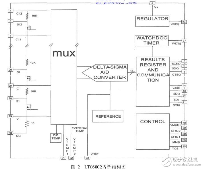
Din 41612 Connector,Din 41612 Vertical Female Connectors,Din 41612 Right Angle Plug Connectors,Din41612 Vertical Plug Press-Fit Connectors
Shenzhen Hongyian Electronics Co., Ltd. , https://www.hongyiancon.com