With the development of modern industrial technology and the continuous improvement of signal processing requirements, data acquisition plays a decisive role for a reliable and stable system. The data acquisition and processing system is widely used. The basic principle is to convert the voltage of the external analog signal into a digital quantity through an A/D converter and store it in the internal RAM. The data is processed through a series of algorithms.
This system uses TI's TMS320F2812 as the core of signal acquisition and processing. It is collected by the MTBSP module external expansion A/D converter LTC1865 of TMS320F2812.
System hardware design TMS320F2812 and its McBSP moduleTMS320F2812 is a high performance, versatile and cost-effective 32-bit fixed-point DSP chip from TI. The chip is compatible with the TMS320LF2407 instruction system and can operate up to 150MHz, with 18K & TImes; 16-bit zero-wait period on-chip SRAM and 128K & TImes; 16-bit on-chip Flash (access time is 36ns). The TMS320F2812 adopts the Harvard bus structure and has a password protection mechanism. It can perform dual 16×16 multiply-add and 32×32 multiply-add operations, providing sufficient processing power to make the application of some complex real-time control algorithms possible, thus having control and fast. The dual function of computing.
The McBSP of the TMS320F2812 chip is a synchronous serial interface that can be configured according to the different needs of the designer and is very flexible to use. McBSP's clock stop mode provides an SPI-compatible protocol. When McBSP is configured for clock stop mode, the transmitter and receiver are not synchronized, so that McBSP can function as an SPI master or slave. In this mode, the transmit clock signal CLKX of McBSP is equivalent to the SCK signal of the SPI bus, and the transmit frame sync signal FSX can be used as the chip select enable signal SS of the SPI. In the clock stop mode, since the internal synchronization mode is employed, the reception clock signal CLKR and the reception frame synchronization signal FSR are not used.
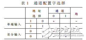
Serial A/D Converter LTC1865The digital-to-analog converter LTC1865 used in this system is a 16-bit SARADC from Linear Technology that operates from a single 5V supply and is guaranteed to operate over the -40°C to +125°C temperature range. Each device maximum meter 1 channel configuration word select single-ended input differential input address selection 10110001 channel 01+-+--+ ground--flow is 850μA, the maximum sampling rate is 250kS/s, the supply current decreases with the sampling rate Become smaller. The LSOP1865 in the MSOP-10 package provides two software programmable channels and the reference voltage can be adjusted as needed. 3-wire SPI-compatible serial interface communication for high-resolution applications such as automotive temperature sensing, engine oil pressure measurement, or Doppler signal acquisition.
The working sequence of LIC1865 is shown in Figure 1. The LTC1865 conversion cycle begins on the rising edge of the CONV signal (ie, when CONV is high), and the conversion ends after a period of tCONV. If CONV is still high at this time, the LTC1865 pulls the supply current low into the power-saving mode. When CONV goes low, two channel configuration bits are input sequentially from the SDI pin on the rising edge of SCK (other input bits are ignored) until the next CONV cycle occurs. Both SCK synchronization and data transmission are in full-duplex mode of operation. After the data is transferred, if CONV is still low, SDO outputs 0 on the rising edge of SCK.

LTC1865's working sequence diagram
The two channel input configuration words determine the channel for the next conversion and its sampling mode. As shown in Table 1, if the configuration word is 10, the LTC1865 will measure the CH0 pin to ground signal; if the configuration word is 11, the LTC1865 will measure the CH1 pin to ground signal; if the configuration word is 00, LTC1865 The signal from the CH0 pin to the CH1 pin will be measured; if the configuration word is 01, the LTC1865 will measure the CH1 pin to the CH0 pin. The LTC1865 samples from VREF to VCC. The voltage of VREF is determined by the pin VREF and can be configured from 1V to VCC by hardware.
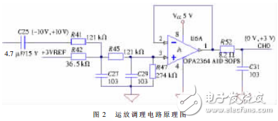
The signal conditioning circuit is an analog signal that amplifies, buffers, or calibrates the sensor, making it suitable for the input of an analog-to-digital converter (ADC). The op amp selected in this system is TI's high CMR (common mode rejection), RRIO (rail-to-rail input and output) OPA2364 chip, which has single power supply, low bias and high performance, which fully conforms to the design of this acquisition system. Claim. Figure 2 shows the circuit schematic of channel 0. To minimize the effects of the acquisition circuit on the sensor, the op amp uses a non-inverting amplifier with high input impedance. The signal is tuned from the op amp's input range ±10V to the input range suitable for the ADC. The principle of channel 1 is the same as channel 0.
The hardware circuit connection of TMS320F2812 and LTC1865 is shown as in Fig. 3. Since the LTC1865 is a 5V power A/D converter and the TMS320F2812 is a 3V chip, the serial data receive pin MDR in the McBSP module of the TMS320F2812 must be passed through the optocoupler TLP512 and the LTC1865 serial data output pin ADSDO. Isolation to prevent burning of the DSP. However, the data transmission direction of McBSP's transmit frame sync pin MFSX, transmit clock pin MCLKXA, and serial data transmit pin MDXA is from DSP to ADC, so no optocoupler is required for isolation.
Dongguan Yijia Optoelectronics Co., Ltd. , https://www.everbestlcdlcms.com