With the improvement of technology and process, the factor limiting the communication distance in the communication system is not the weak degree of the signal, but the degree of noise interference. Overcoming noise interference is an issue that must be considered when designing electronic devices. In a broad sense. Noise refers to unwanted interference signals in the design. However, various communication signals are usually transmitted in the form of electric waves. Therefore, while receiving useful signals, various unwanted signals are inevitably mixed. Even if filtering, shielding, etc. are adopted, there will be more or less useless signals infiltrating into the receiving channel, interfering with subsequent signal processing. While improving external interference, it is also necessary to give full play to the designer's subjective initiative, that is, to reduce the device's own interference from the inside of the receiver, mainly using a low-noise amplifier. Therefore, a design scheme of a low noise amplifier is proposed here.
1 Low noise amplifier technical indicators and design principles1.1 Main technical indicators
The main technical specifications of the low noise amplifier include: noise figure, power gain, input-output standing wave ratio, reflection coefficient and dynamic range. Since the low noise amplifier is designed, the noise figure is mainly considered while taking into account other indicators. The noise figure is the signal-to-noise ratio that is degraded by the noise generated by the amplifier (or microwave device) after the signal passes through the amplifier (or microwave device). The multiple of the signal-to-noise ratio reduction is the noise figure, usually expressed in NF. The noise generated by the amplifier itself is usually expressed as the equivalent noise temperature. Relationship between noise temperature and noise figure NF
![]()
Where T0 is the ambient temperature, usually in absolute temperature, 293 K. Note: The noise figure NF here is not in dB.
For a single-stage amplifier, the noise figure is calculated as
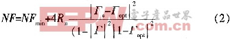
In the formula, NFmin is the minimum noise figure of the transistor, which is determined by the transistor itself; Γout, Rn, Гs are the optimal source reflection coefficient when obtaining NFmin, the equivalent noise resistance of the transistor, and the source reflection coefficient at the input end of the transistor.
The multi-stage amplifier noise figure is calculated as
![]()
In the formula, NF is always the noise figure of the whole amplifier; NF1, NF2, and NF3 are the noise coefficients of the first, second, and third levels, respectively; G1 and G2 are the first and second power gains, respectively.
It can be seen from equation (3) that when the current stage gains G1 and G2 are sufficiently large, the noise figure of the whole machine is close to the noise figure of the first stage. Therefore, in the multi-stage amplifier, the magnitude of the noise figure of the first stage plays a decisive role.
1.2 Design principles
1.2.1 Selection of transistors
The main technical specifications of low noise transistors in RF circuits are: high gain, low noise, and sufficient dynamic range. At present, the operating frequency of the bipolar low-noise tube can reach several tens of gigahertz, the noise figure is several decibels, the operating frequency of the gallium arsenide small-signal FET is higher, and the noise figure can be less than 1 dB.
When selecting a low-noise transistor, the following two principles are generally followed: 1) The noise figure of the microwave low-noise transistor is sufficiently small, and the operating frequency band is sufficiently high. In general, the fT of the selected transistor is more than 4 times higher than its operating frequency; 2) The selected microwave low noise transistor should have a sufficiently high gain and a sufficiently large dynamic range. The operating gain of the amplifier is usually required to be greater than 10 dB. When the input signal reaches the maximum value of the system, the intermodulation component caused by the nonlinearity of the amplifier is smaller than the system noise.
1.2.2 Circuit Design Principles
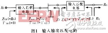
The circuit design principle here is actually the design principle of the input and output matching circuit. First, the design principle of the input matching circuit is to increase the circuit gain under the premise that the minimum noise is preferentially satisfied. That is, the appropriate Гout is selected according to the input gain circle and the equal noise circle. As shown in Figure 1, Zout = Zopt, Гout = Гopt is usually required. Second, the basic task of the output matching circuit is to match the complex output impedance of the microwave tube to a load real impedance of 50 Ω. The output matching circuit mainly improves the gain, so the designed output matching circuit can achieve its task when Zin=ZT* is established. Furthermore, the amplifier design must be such that the designed amplifier is stable, that is, it needs to meet stability conditions. Finally, while meeting the indicators, focus on process and structural achievability. The process should select a printed board with low loss, easy processing, stable properties, uniform physical (thickness) and electrical properties (dielectric constant) of the material, and a surface finish to meet certain requirements. For the substrate material, FR-4 (between dielectric constants 4 and 5) and alumina ceramics are commonly used microwave substrates. It is also necessary to consider the influence of adjacent related circuits when laying out the PCB. In addition, attention should be paid to the principles of electromagnetic compatibility design in filtering, grounding, and external circuit design.
The design was designed with the help of the powerful RF circuit design and simulation software ADS. The low-noise amplifier designed here is the simplest single-stage low-noise amplifier designed to simplify the design of low-noise amplifiers using computer-aided design software.
2.1 Indicator requirements
In order to clearly illustrate the design process of the low noise amplifier, the design specifications are not very high, as follows: frequency range is 2 ~ 2.2 GHz; gain G is greater than 15 dB: noise figure NF is less than 1 dB; operating voltage is 5 V Operating current less than 150 mA: input and output standing wave ratio VSWR is less than 1.5; input and output impedance is 50 Ω; RF signal connector is SMA; external dimensions are 43 mm x 26 mm x 8 mm.
2.2 Design steps
2.2.1 Transistor selection
Agilent's ATF-54143 transistor was chosen here by reviewing the relevant information from the transistor manufacturer and synthesizing the selection principle of the above-mentioned low-noise transistor.
2.2.2 The topology is sufficient
After selecting the transistor, it is theoretically necessary to determine the DC operating point. However, in actual engineering practice, the corresponding S-parameters in the data of the selected transistor are directly written into the corresponding design software, and the S-parameter is used as the analog design circuit. The S parameter can fully reflect all the characteristics of the transistor because: 1) When the internal structure of the device is not concerned, only the external characteristics can be used to replace the external characteristics of the device in the form of network parameters; 2) Transistors The relevant parameters of the data are measured for the actual product under a certain experimental platform, so it is closer to the actual characteristics of the device.
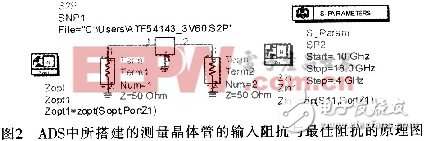
Figure 2 shows the circuit built into the ADS for the selected transistor. It is mainly used to measure the input impedance of the transistor and the optimum impedance corresponding to the minimum noise figure. These measurements are easily implemented in ADS.
The input matching network is designed based on the above input impedance results. This design meets the minimum noise match and takes into account the gain specification. The reason for this can be obtained by the formula (3). The PHEMT transistor is chosen here, which enables a low noise figure when the noise figure is not minimal.
In the design process, we tried to aim at the minimum noise matching, but finally chose the optimal gain matching as the target design under the premise of gain. However, whether it is aimed at minimum noise or maximum gain matching, the implementation in ADS is basically the same.
After determining the matching target, the ADS design wizard can be easily used to design the matching circuit. Usually the branch is matched. When the single-branch module in the design wizard is selected, the preset matching circuit can be easily realized by setting the input and output matching parameters. As shown in Figure 3. 3(b) is a specific form of the microstrip branch matching in FIG. 3(a). It should be noted here that the substrate material selected during the design process is epoxy glass FR-4 with a dielectric constant of 4.3 and a substrate thickness of 0.8 mm.
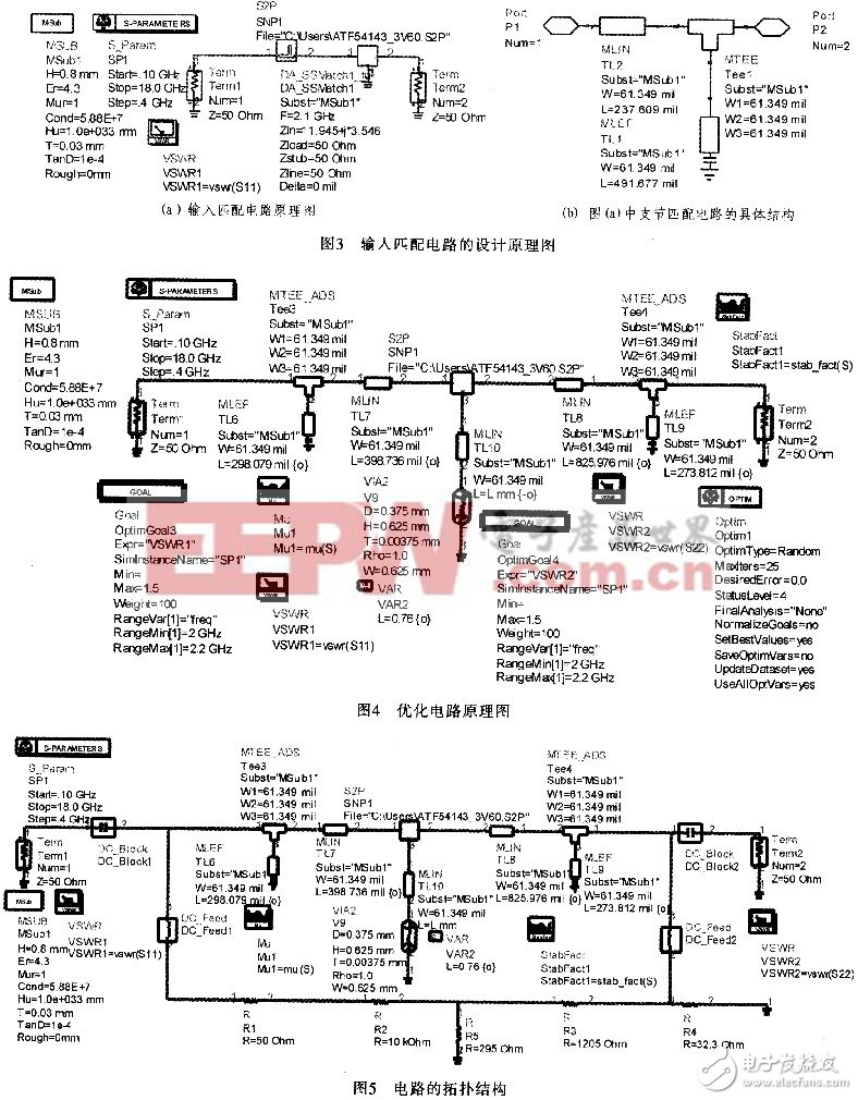
After the design of the input matching circuit is completed, the next step is to design the output matching circuit, and use the similar method to the input matching circuit design to obtain the initial value of the output matching circuit. The reason why this is the initial value is because when the output matching circuit is designed according to the target value, the input standing wave ratio does not meet the index requirement. Therefore, the output matching circuit must be adjusted accordingly. In order to give full play to the advantages of CAD software, the adjustment of the matching circuit is by means of the optimization method, and FIG. 4 is the schematic diagram of the optimization circuit.
Finally, the bias network is used for the overall simulation. In fact, the addition of the offset network does not have a great impact on the simulation process. Because the bias network is connected through the high-frequency choke, the RF signal does not affect the power supply portion, and the power is introduced through a quarter-wavelength transmission line. Therefore, for the RF circuit, the access point of the power supply to the RF circuit is equivalent to opening the RF signal. Similarly, the introduction of the DC power supply does not affect the RF circuit, and the DC block is also added to the input of the RF signal. , further blocking the DC pair
The impact of RF signals. The topology of the final circuit is shown in Figure 5.
3 Design results3.1 Simulation results
The low noise amplifier design results are shown in Figure 6. It can be seen from Figure 6 that the input-output standing wave ratios VSWR1 and VSWR2 are less than 1.5 in the entire frequency band: the gain is greater than 15 dB in dB(S(2,1)), and the noise figure nf(2) is less than 0.5. The stability factor StabFactl and the stability factor are both greater than 1, which means that the designed low noise amplifier fully meets the requirements of the index.

3.2 Design results of the layout
Using ADS, the characteristics of the layout can be generated directly from the schematic. First, the layout is produced from the completed schematic in ADS. Through the corresponding adjustment of the layout, the layout and structure design are completed in the form of AutoCAD. The result is shown in Figure 7. Show.

It can be easily seen from Figure 7 that in the layout design, many small squares are placed on both sides of the microstrip line, which are fine-tuning islands that are often used in microwave circuit design. Although the adjustment is limited, with these fine-tuning islands, the design cost can be saved to a certain extent: there is not enough adjustment to the board, and it is not enough to be fine-tuned and needs to be reprinted. The application of the fan-shaped routing in the layout plays a role in adjusting the gain flatness: for some lower frequency signals, the fan-shaped path shorts these signals, thereby reducing the gain of the low-end signal. The fan-shaped structure can greatly increase the adjustment range. A supplementary point to the structure is that the narrow side of the box must be less than one-half the wavelength of the highest frequency of the operating band. This requirement is limited by the theory of the cut-off waveguide.
4 ConclusionThe design flow of the entire low noise amplifier is discussed through the design and simulation of a simple low noise amplifier. In particular, how to implement low-noise amplifiers in ADS is discussed in detail, which fully demonstrates the advantages of computer-aided design. In the design of the matching circuit, the open-circuit branch matching circuit is adopted; in the design of the layout, the content of the sector-shaped open-section branch is also reflected in the theory of quarter-wave impedance transformation; the deadline is also involved in the structural design. The application of waveguide-related theory fully embodies the perfect combination of theory and practice.
Insulated Copper Tube Terminals
Insulated Copper Tube Terminals,High quality insulated terminal,copper tube terminal
Taixing Longyi Terminals Co.,Ltd. , https://www.lycopperlugs.com