With the development of microelectronics technology and computer technology, the electrical equipment, which is mainly based on strong electricity and electrical appliances, has become a new type of microelectronic equipment with strong digital characteristics and complete functions. On many occasions, more and more single-chip products have emerged to replace traditional electrical control products. The single-chip microcomputer belonging to the memory program control has its control function realized by software instructions, and its hardware configuration is also variable and variable. Therefore, once the production process changes, it is not necessary to redesign the line connection installation, which is conducive to product replacement and order production.
The various control signals used in conventional electrical equipment must be converted to digital signals that match the input/output ports of the microcontroller. The user equipment must input various control signals to the single-chip microcomputer, such as limit switches, operation buttons, selection switches, travel switches, and other switching outputs of the sensors, etc., and convert them into signals that can be received and processed by the single-chip microcomputer through the input circuit. The output circuit should convert and amplify the weak electric control signal sent by the single-chip microcomputer to the strong output signal required by the field to drive the actuators of the power tube, solenoid valve and relay, contactor, motor and other controlled devices, which can facilitate the actual control system. . In view of the characteristics of electrical control products, this paper discusses the design methods of common drive and isolation circuits for several kinds of single-chip I/O. It has practical to design the electrical control system reasonably, improve the interface capability of the circuit, and enhance the stability and anti-interference ability of the system. Guiding significance.
1, input circuit design
 Figure 1 Switch signal input
 Generally, the input signal will be input into the MCU in the form of a switch. From the engineering experience, the effective state of the control input of the switch input is much better than the high level effect, as shown in Figure 1. When the switch S1 is pressed, the command signal sent is low level, and when the switch S1 is not pressed normally, the level outputted to the single chip is high. This method has strong noise resistance.
If it is considered that the TTL level voltage is low and it is susceptible to external interference in long-line transmission, the input signal can be increased to +24 V, and the high-voltage signal is converted into a TTL signal at the entrance of the microcontroller. This high-voltage transmission method not only improves the noise resistance, but also makes the contact of the switch contact good and reliable, as shown in Figure 2. Among them, D1 is a protection diode, and the reverse voltage is ≥50 V.
 Figure 2 Increase the input signal level
 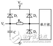 Figure 3 input protection circuit
 In order to prevent external spikes and static electricity from damaging the input pins, an anti-pulse diode can be added to the input to form a resistor bidirectional protection circuit, as shown in Figure 3. The forward voltage drop UF 二æžç®¡ 0.7 V of the diodes D1, D2, and D3, and the reverse breakdown voltage UBR ≈ 30 V, the protection circuit can limit the amplitude of the voltage regardless of the polarity of the input voltage at the input end. The input can withstand the range. That is: when a positive pulse occurs from VI to VCC, D1 is forward-conducting; when a negative pulse occurs from VI to VCC, D2 reverse-breaks; when a positive pulse occurs between VI and ground, D3 reverse-breaks; between VI and ground When a negative pulse occurs, D3 is forward-conducting and the diode acts as a clamp. The snubber resistor RS is about 1.5 to 2.5 kΩ, and forms an integration circuit with the input capacitor C, delaying the external induced voltage for a period of time. If the existence time of the interference voltage is less than Ï„, the effective voltage applied to the input terminal will be much lower than its amplitude; if the time is longer, D1 is turned on, and the current forms a certain voltage drop on the RS, thereby reducing the input voltage value.
In addition, a common input method is to use an optocoupler isolation circuit. As shown in Figure 4, R is the input current limiting resistor, limiting the LED current in the optocoupler to 10-20 mA. The input is coupled by an optical signal and is electrically isolated completely. At the same time, the forward resistance of the LED is low, and the internal resistance of the external interference source is generally high. According to the principle of voltage division, the interference noise that the interference source can feed to the input terminal is small, and no ground interference or other crosstalk is generated. Enhanced the anti-interference ability of the circuit.
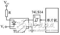 Figure 4 Input optocoupler isolation
 Under the premise of satisfying the function, the simplest solution to improve the reliability of the input end of the MCU is: Connect a capacitor in parallel with the input to the ground to absorb the interference pulse, or connect a metal film resistor in series to limit the peak current flowing into the port.
2, the output circuit design
The output port of the MCU is limited by the driving capability. Under normal circumstances, a dedicated interface chip is required. Although the output varies greatly depending on the control object, it generally meets the requirements of output voltage, current, switching frequency, waveform rising and falling rate and isolation anti-interference. Here are some typical circuit implementation methods for the output from the microcontroller to the power.
2.1 Direct coupling
In the output circuit using direct coupling, the circuit shown in Figure 5 should be avoided.
 Figure 5 Wrong output circuit
 During the T1 turn-off and T2 turn-on period, in order to provide sufficient base current to T2, the resistance of R2 must be small. Since T2 operates in the emitter follower mode, in order to reduce the T2 loss, the voltage drop between the collectors must be controlled to a small range. In this way, the voltage between the bases is also small, and the resistance of the resistor R2 is small to provide sufficient base current. If the resistance of R2 is too large, it will greatly increase the pressure drop of T2, causing serious heat generation of T2. During the T2 cut-off period, T1 must be turned on, and the high voltage +15 V is all dropped on the resistor R2, which generates a large current, which is obviously unreasonable. In addition, the conduction of T1 will cause the high-level output of the microcontroller to be pulled down to near ground potential, causing the output to be unstable. The base of T2 is pulled to ground potential by T1. If it is followed by an inductive load, due to the back EMF of the winding, the emitter of T2 may have a high level, which may cause reverse breakdown of the T2 tube base.
Figure 6 shows a direct coupled output circuit with a coupling circuit composed of T1 and T2 to drive T3. When T1 is turned on, a current is generated in the series circuit of R3 and R4, and the voltage division on R3 is greater than the base emitter junction voltage drop of the T2 transistor, which causes T2 to be turned on, and T2 provides the base current of the power tube T3, so that T3 is made. It becomes conductive. When the T1 input is low, T1 is turned off, the voltage drop on R3 is zero, T2 is turned off, and finally T3 is turned off. The role of R5 is as follows: On the one hand, as a load of the T2 collector, on the other hand, when T2 is turned off, the charge stored in the base of T3 can be quickly released through the resistor R3, which accelerates the cut-off speed of T3 and is beneficial to reduce the loss.
 Figure 6 Direct coupled output circuit
 2.2 TTL or CMOS device coupling
If the microcontroller is output via TTL or CMOS chip, the device with open collector is generally used, as shown in Figure 7(a). The open collector device is connected to the +15 V supply through the collector load resistor R1, which boosts the drive voltage. However, it should be noted that the switching speed of this circuit is low. If the power transistor is directly driven, when the subsequent circuit has an inductive load, the phase relationship of the power tube will affect the waveform rise time, resulting in dynamic loss of the power tube. Increase.
In order to improve the switching speed, two improved output circuits can be used, as shown in Fig. 7(b) and Fig. 7(c). Figure 7(b) shows an improved circuit that can be quickly turned on. When the TTL output is high, the output point obtains voltage and current through transistor T1, and the charging capability is increased, thereby speeding up the turn-on speed and also reducing the open-collector TTL device. Power consumption. Fig. 7(c) shows a push-pull improved circuit. This circuit not only improves the speed at turn-on, but also increases the speed at turn-off. The output transistor T1 operates as an emitter follower without saturation and thus does not affect the output switching frequency.
 Figure 7 TTL or CMOS device output circuit
 2.3 Pulse transformer coupling
The pulse transformer is a typical electromagnetic isolation component. The switching signal output by the single chip is converted into a carrier signal with a high frequency and coupled to the output stage via a pulse transformer. Since there is no circuit connection between the primary and secondary coils of the pulse transformer, the output is a level floating signal, which can be directly coupled with a high voltage component such as a power tube, as shown in FIG.
 Figure 8 pulse transformer output circuit
 This circuit must have a pulse source. The frequency of the pulse source is the carrier frequency and should be at least 10 times higher than the output frequency of the microcontroller. The output pulse of the pulse source is sent to the control gate G, and the output signal of the single chip is input to the G gate from the other end. When the MCU outputs a high level, the G gate is opened, and the output pulse enters the transformer. The secondary coil of the transformer outputs a pulse of the same frequency as the primary side. After being detected by the diodes D1 and D2, it is filtered to be converted into a switching signal and sent to the power tube. When the MCU outputs a low level, the G gate is closed, the pulse source cannot enter the transformer through the G gate, and the transformer has no output.
Here, the transformer transmits both the signal and the energy, which increases the frequency of the pulse source and helps to reduce the weight of the transformer. Since the transformer can adapt to different driving power requirements by adjusting the inductance, the number of primary and secondary turns, etc., it is more flexible to apply. More importantly, there is no electrical connection between the primary and secondary coils of the transformer, and the secondary coil output signal can float following the voltage of the power component, independent of the size of its power supply.
When the MCU outputs a pulse signal of a higher frequency, the pulse source and the G gate may not be used, and the original secondary circuit of the transformer may be appropriately adjusted.
2.4 Photoelectric coupling
Optocoupler can transmit linear signals as well as transmit switching signals, which are mainly used to transmit switching signals during output stage applications. As shown in FIG. 9, the MCU output control signal is amplified by the buffer 7407 and sent to the optocoupler. R2 is the load resistance of the optocoupler output transistor. It should be selected to ensure that the output transistor is reliably saturated when the optocoupler is turned on, and T1 is reliably saturated when the optocoupler is turned off. However, due to the slow response of the optocoupler, the switching delay time is lengthened, which limits its frequency of use.
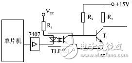 Figure 9 optocoupler output circuit
 Conclusion
The interface technology of single-chip microcomputer has been introduced in detail in many literatures. However, in the transformation and design of a large number of electrical control products, problems that cannot be solved by interface chips are often encountered (such as large drive current, slow switching speed, anti-interference). Poor, etc., so another circuit solution must be sought. The above several input/output circuits have been shown by a wide range of applications, which have high engineering practical value for the reasonable and reliable implementation of the single-chip electrical control system.
Spring Fingers,Shielding Case
ShenZhen Antenk Electronics Co,Ltd , https://www.antenkconn.com