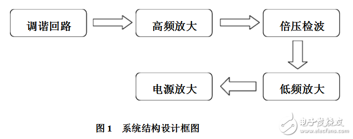
The basic working principle of the radio can be simply summarized as follows: the first step is to receive the radio wave of the corresponding frequency, the second step is to take out the sound information modulated on it from the radio wave, and the third step is to restore the sound information to human ear energy The sound heard. As shown in Figure 1, a simple radio system consists of five modules. After the tuning signal is selected by the tuning loop, the received radio signal is very weak. After passing through the tuning circuit, it needs to be amplified by the high-frequency amplifier circuit to a certain amplitude before it can be sent to the diode and filter capacitor. The voltage doubler detection circuit detects and demodulates the amplitude-modulated signal envelope to obtain the audio signal in front of the modulation. The audio signal is amplified at a low frequency. The sound information is still an electrical signal with a very low amplitude at this time. Unexpectedly, after the transistor current is amplified, it is sent to the speaker and restored to an audible sound wave signal.
The simple radio is very simple to make. It can receive simple radios in the middle section of 550kHz to 1600kHz by changing the size of inductance and capacitance. And the audio output of the radio basically reaches the level that the human ear can hear.
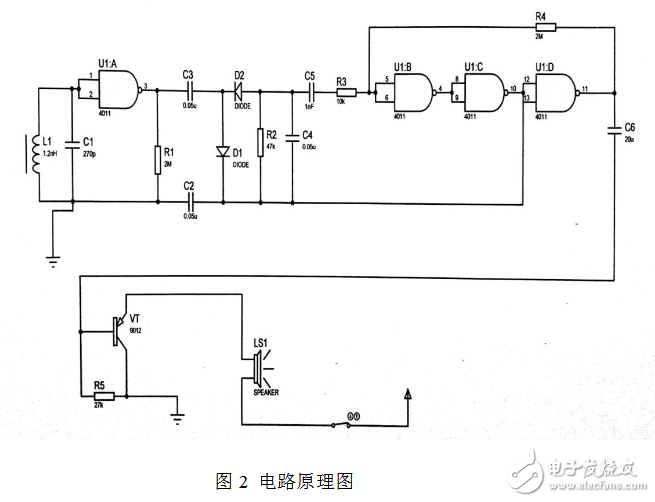
According to the basic working principle of the above radio, the chip CD4011 is used to design the circuit diagram of the working principle of the simple radio as shown in FIG. 2.
2. Analysis of circuit working principle
The circuit diagram is shown in Figure 2. Under normal circumstances, this type of NAND gate circuit is made in two states of on and off, that is, output high level and low level. In fact, during the transition between high and low levels, there is a transition zone, and the middle part of the transition zone is basically linear. Therefore, the feedback circuit can be used to select an appropriate working state so that each NAND gate is in an amplified state. The circuit and working principle are shown in Figure 2. The input terminals of each NAND gate are connected in parallel as an inverter, and the high and low levels are converted. L1, C1 is the receiving resonant circuit, R1 is the DC feedback resistor, C2 is the AC bypass function, the received signal is amplified by U1A high frequency, coupled through C3, and sent to the voltage doubler detection composed of D1, D2, R2, C4 The circuit performs detection, and then further amplified by the gate U1B, U1C, U1D and sent to the headphone output. C1 on the way can choose a single string of variable capacitors. The coil L can be wound around a 50MM magnetic bar for 80 ~ 100T. The headphones should use high-impedance headphones, or a level one integrated audio amplifier circuit such as LM386, or a triode for impedance transformation, By increasing and decreasing the number of turns of the coil on the magnetic bar, to ensure that the radio is within the appropriate frequency reception range.
Note: (1) CD4011: 4-2 input NAND digital integrated circuit.
(2) The model of variable capacitor is CBM-233P, and the capacitance varies between 5 ~ 141p. The inductance coil L is wound with 100 turns on a magnet rod of enameled wire 5 * 3 * 55mm with a diameter of 0.18mm. The triode uses 9012. The power supply uses 4 No. 5 batteries. The headphones use 32 ohm stereo headphones.
3. Analysis and introduction of the working principle of each module
(1) Tuning loop module
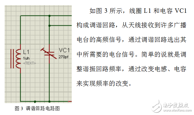
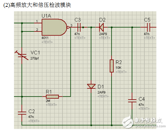
Figure 4 High-frequency amplification and voltage doubler detection circuit diagram
As shown in Fig. 4, there is a NAND gate CD4011 that performs high-frequency amplification, and then a voltage doubler detection circuit composed of diodes D1, D2, capacitor C3, and resistor R2 performs detection. When the signal voltage is positive half cycle, the signal voltage enters D1 to charge C3, and the voltage on C3 is left positive and negative. When the signal voltage is negative half cycle, the signal voltage and C3 are connected in series and flow through the diode D2 and the resistor R2. The output voltage of the detection load resistor R2 is about twice that of the signal voltage. The function of the capacitor C4 is to filter the detection output signal. High-frequency components in the audio signal.
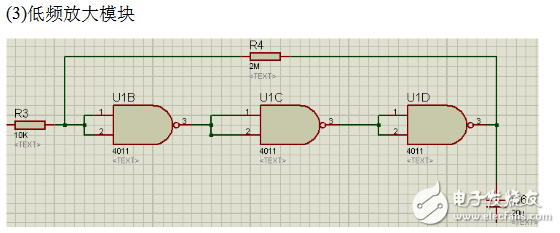
Figure 5 Low frequency amplification circuit diagram
As shown in Figure 5, the CMOS analog amplifier circuit adds an appropriate bias voltage to the CMOS gate circuit, which can make it work in a linear amplification state. A feedback resistor R4 is connected in parallel between the output terminal and the input terminal of the NAND gate CD4011, and the operating point of the NAND gate is biased in the middle of the transfer characteristic curve, that is, a linear analog amplifier is formed, and the amplification factor is equal to the feedback resistor R4 Ratio with input resistance R3.
(4) Power amplifier module
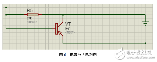
As shown in Figure 6, because the output current of the CMOS circuit is very small, in order to make the radio have sufficient volume, the circuit is constructed by a transistor VT a primary current amplifier, R5 is the bias resistance of the transistor VT. The current amplification module is essentially an emitter follower, which can amplify the output current of the CMOS circuit.
4. [Analysis of Simulation and Simulation Results]
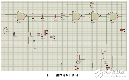
As shown in Figure 7 is the overall circuit simulation diagram. After the simulation, the speaker can hear the buzzing sound. According to the principle, the size of the inductance can be changed to receive the radio station in the middle band of 535kHz to 1065kHz, but after adjustment, it has never received the effective frequency band. sound. Therefore, the simulation test of the design module is carried out. (1) Low frequency amplification simulation
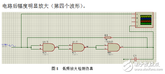
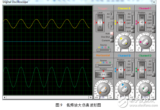
As shown in Figure 8, an AC signal source is connected to the left side, and an oscilloscope is connected to the other end of the amplifier circuit. As can be seen from Figure 9, the input signal (the first waveform) is amplified
(2) Power supply amplification simulation
As shown in Figure 10, connect an AC signal source on the left and connect an oscilloscope to the other end of the amplifier circuit. From Figure 11, you can see the input signal (first waveform) and output signal (fourth waveform) ).
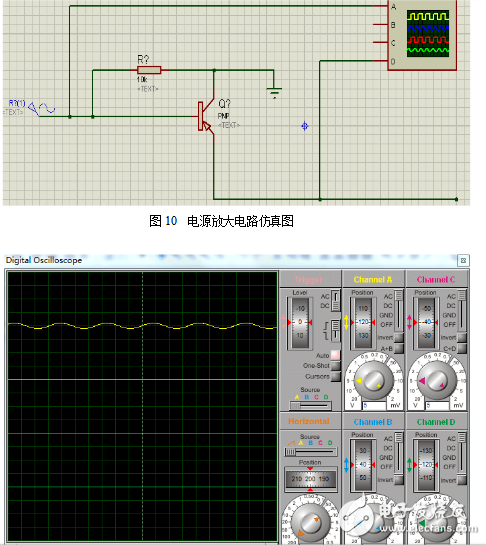
Figure 11 Simulation waveform before power amplification
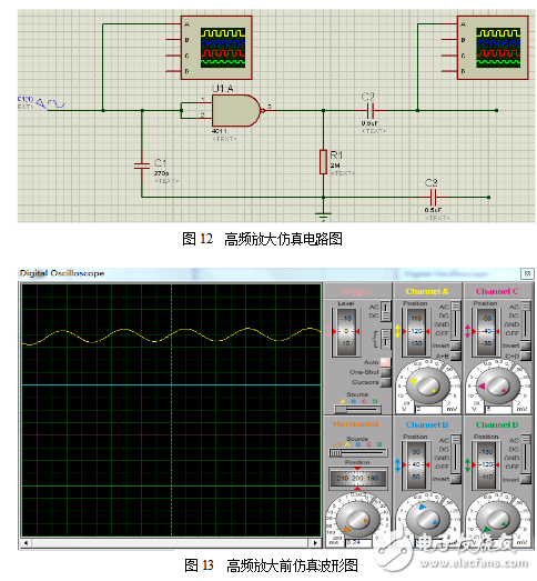
(3) High frequency amplification simulation
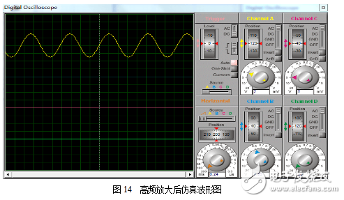
The simulation circuit diagram is shown in Figure 12. Connect an AC signal source on the left side, and then connect two oscilloscopes to both ends of the circuit. The waveform shown in Figure 13 is amplified by the amplifier circuit and the waveform is shown in Figure 14. It can be seen that the amplitude of the signal increases significantly after being amplified.
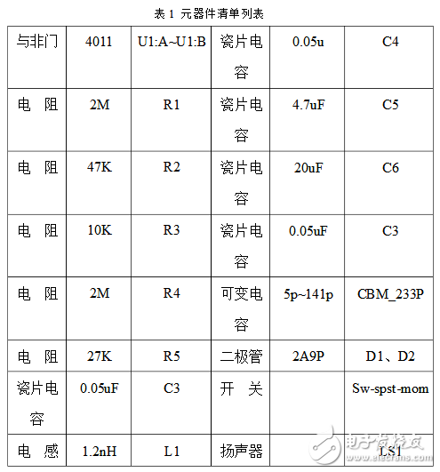
5. [Components List]
to sum up
Through the design of the CD4011 chip to make a simple radio, I learned the working principle of the radio, truly understood the modulation and demodulation process, and also understood the function and use of the pins of the CD4011 chip.
Improve ideas
During simulation, the circuit element CD4011 in the circuit diagram is not found in Proteus, so NAND gate 4011 is used instead. Since CD4011 is a CMOS circuit containing 4 NAND gates, each NAND gate has two inputs One output. When one of the two input terminals is 0, the output is 0. Only when both inputs are 1, the output is 1. When both inputs are 0, the output is 1. So CD4011 is replaced by 4011 in the picture. The high-frequency antenna signal obtained by the simple radio from the receiving antenna is generally very weak. Even if a high-frequency amplifier has been added, the power of the detection output is usually only a few milliwatts. You can still listen to it with headphones, but it seems too small to use the speaker. After detecting the output, a current amplifier is added to push the speaker to work. If a superheterodyne circuit is used, the local oscillator frequency of the radio differs from the frequency of other received signals by an intermediate frequency. The selection circuit and the local oscillator before the mixer use a uniform tuning line. Because the intermediate frequency is fixed and the frequency is adjusted higher than the high frequency The signal is low, the gain of the Chinese side can be made larger, the work is relatively stable, and the passband characteristics can also be made ideal, so that the detector can obtain a sufficiently large signal, so that the sound quality of the entire simple radio is better. audio signal.
KNL5-100 Residual Current Circuit Breaker
KNL5-100 Moulded Case Circuit Breaker is MCCB , How to select good Molded Case Circuit Breaker suppliers? Korlen electric is your first choice. All moulded Case Circuit Breakers pass the CE.CB.SEMKO.SIRIM etc. Certificates.
Moulded Case Circuit Breaker /MCCB can be used to distribute electric power and protect power equipment against overload and short-current, and can change the circuit and start motor infrequently. The application of Moulded Case Circuit Breaker /MCCB is industrial.
Korlen electric also provide Miniature Circuit Breaker /MCB. Residual Current Circuit Breaker /RCCB. RCBO. Led light and so on .
KNL5-100 Molded Case Circuit Breaker,KNL5-100 Small Size Molded Case Circuit Breaker,KNL5-100 Electrical Molded Case Circuit Breaker,KNL5-100 Automatic Molded Case Circuit Breaker
Wenzhou Korlen Electric Appliances Co., Ltd. , https://www.zjmotorstarter.com