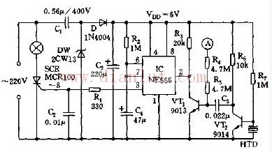
The schematic diagram of the touch and voice control dual function delay lamp circuit is shown in the figure. In the figure, Cl, C2, VD, and VS form a capacitor step-down half-wave rectification voltage regulator circuit. After power-on, C2 can output DC voltage of about 12V for 555 time base integrated circuit power. The 555 time-base integrated circuit is connected to a typical monostable flip-flop. The normal circuit is in a stable state, the 3-pin output is low, the thyristor VTH is turned off, and the EL is not lit. When you need to turn on the light, you can use the touch method or the voice control method. If the electrode piece M is touched by hand, the leakage current of the human body is injected into the base of VT1 through R5, and VTl is turned on, that is, a negative pulse is input to the 2 pin of the 555 time base integrated circuit, and the 555 time base integrated circuit is put into the temporary position. Steady state, 3 feet output high level, VT3 is turned on, the electric lamp EL lights up and emits about lmin. If the voice control method is used, the palm can be hit, and the piezoelectric ceramic piece B converts the received sound wave signal into a corresponding electrical signal. After two stages of amplification by VI2 and VTl, the 555 time base integrated circuit can also be turned over and set. The electric lamp EL is lit. After about 1.1R, C3, the potential of 6 feet rises to the end of 2VD transient steady state, the circuit returns to the original stable state, the 3 pin outputs low level, VT3 turns off when the alternating current crosses zero, and the electric lamp EL goes out.
Since the electrolytic capacitor capacity is mostly positive, and the leakage current factor is added, the actual delay time is larger than the calculated value. The data shown in the figure is used, and the delay time is about 1 min. The function of C3 is anti-interference, which can prevent grid voltage fluctuations and the false triggering of the interference pulse caused by switching other household appliances to this circuit.
C1 requires a withstand voltage of 400V or higher, and R5 must use a high resistance resistor.
VTl and VT2 use 9014 silicon NPN transistor, which requires current amplification factor β>200.
B can use Φ27mm piezoelectric ceramic piece, and make resonance chamber for it to increase the sensitivity of receiving sound waves. There should be plastic mesh cover on the outside of the piezoelectric ceramic piece, so that the human hand can not directly contact with it to ensure the safety of the user. .
There are no special requirements for other components, and the models and parameters are selected according to the drawings.
For industrial control environment wired communication equipment and wireless communication equipment. Wired communication equipment mainly introduces serial equipment communication for industrial field, professional bus-type communication, industrial Ethernet communication and conversion equipment between various communication protocols, including routers, switches, modems and other equipment. Wireless communication equipment mainly includes wireless AP, wireless bridge, wireless network card, wireless lightning arrester, antenna and other equipment. Communications also include military communications and civilian communications
Communication Pcb,Wireless Communication Pcb,Optical Communication Circuit Board,Printed Communication Circuit Boards
Chuangying Electronics Co.,Ltd , https://www.cwpcbs.com