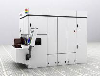
Mask Aligner: Mask aligner, exposure system, lithography system, etc. The general lithography process is subject to processes such as cleaning, drying, coating, spin coating, soft bake, alignment exposure, post-baking, developing, hard-baking, and etching.
Photolithography means the use of light to make a pattern (process); the process of sizing on the surface of a silicon wafer and then transferring the pattern on the mask to the photoresist temporarily “replicates†the device or circuit structure to the wafer On the process.
The purpose of photolithographyMakes the surface hydrophobic and enhances the adhesion of the substrate surface to the photoresist.
Lithography machine working principle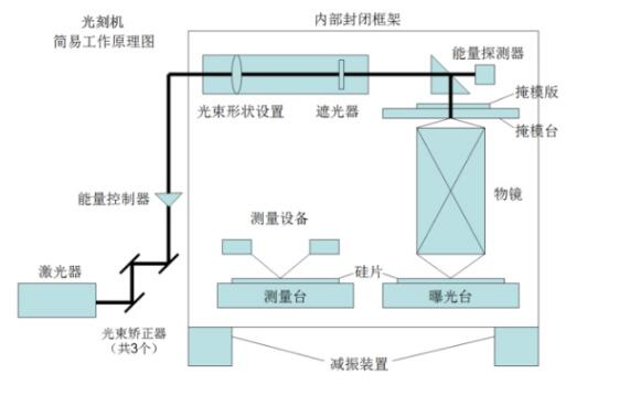
The figure above shows a simplified schematic of a photolithography machine. Below, briefly introduce the role of each device in the figure.
Measuring table, exposure table: Workbench carrying silicon wafers, also known as the double table.
Beam Corrector: Correct the incident direction of the beam and make the beam as parallel as possible.
Energy Controller: Controls the energy that will eventually shine on the silicon wafer. Underexposed or overexposed will seriously affect the imaging quality.
Beam shape setting: Set the beam to round, ring and other shapes, different beam states have different optical characteristics.
Shutter: Blocks the beam from shining on the wafer when exposure is not needed.
Energy detector: Detects whether the final incident energy of the beam meets the exposure requirements and feeds it back to the energy controller for adjustment.
A mask plate: A glass plate engraved with a circuit diagram on the inside, costing hundreds of thousands of dollars.
Masking station: The equipment that carries the motion of the mask, the motion control accuracy is nm level.
Objective: The objective lens is composed of more than 20 lenses. Its main function is to scale down the circuit board on the mask, and then it is laser-mapped on the silicon wafer. The objective lens also compensates for various optical errors. The technical difficulty lies in the difficulty of designing the objective lens and the high precision requirements.
Wafer: A wafer made of silicon crystal. There are many sizes of silicon wafers, and the larger the size, the higher the yield. Digression, because the wafer is round, so need to cut a gap in the silicon wafer to confirm the wafer's coordinate system, according to the shape of the gap is divided into two different, respectively called flat, notch.
Internal closed frame and shock absorber: isolate the work table from the external environment, maintain the level, reduce the external vibration interference, and maintain a stable temperature and pressure.
The lithography machine is generally divided into three types according to the simplicity of operation, manual, semi-automatic, and fully automatic.
A manual: refers to the adjustment of the alignment method, by adjusting the X-axis, Y-axis and thita angle to complete the alignment by hand-tune the knob, the accuracy of the alignment can be imagined and not high;
B semi-automatic: refers to the alignment can be adjusted by the CCD based on the electric axis;
C Automatic: Refers to uploading and downloading from the substrate. The exposure duration and cycle are controlled by the program. The automatic lithography machine mainly meets the factory's need for throughput.
The lithography machine can be divided into three categories: proximity lithography, direct-write lithography, and projection lithography. Proximity contact passes through infinity and copies the pattern on the mask. Projection lithography uses the projection objective to project the structure on the mask onto the surface of the substrate. In direct writing, the beam is focused to a point through the moving workpiece stage or Lens scanning for arbitrary graphics processing. Optical projection lithography has always been a mainstream lithography technology for integrated circuits due to its high efficiency and non-destructive advantages.
Lithography applicationThe lithography machine can be widely applied to the fabrication of micro-nanostructure devices such as micro-nanofluidic wafer processing, micro-nano optical elements, micro-nano gratings, and NMEMS devices.
What is the etching machineIn fact, in a narrow sense, photolithography is used to etch the photoresist by photolithography, and then the other parts of the photoresist are removed by etching. With the development of micro-manufacturing technology, in a broad sense, etching has become a generic term for stripping and removing materials through solution, reactive ions, or other mechanical means, and has become a universal name for micro-fabrication manufacturing.
Inductively coupled plasma etching (ICPE) is the result of a combination of chemical processes and physical processes. Its basic principle is that under the vacuum low pressure, the RF output generated by the ICP RF power supply is output to the ring coupled coil, and a certain proportion of the mixed etching gas is coupled to the glow discharge to generate a high-density plasma, and the RF is applied to the lower electrode. Next, these plasmas bombard the surface of the substrate. The chemical bonds of the semiconductor material in the pattern area of ​​the substrate are broken. Volatile substances are generated with the etching gas, which are released from the substrate in the form of gas, and are drawn away from the vacuum line.
The difference between the etching machine and the lithography machineEtching relative to photolithography is easy.
The lithography machine prints the pattern, and then the etcher etches the patterned (or unpatterned) portion according to the printed pattern, leaving the remaining portion.
Lithography machine related articles:
Lithography machine structure composition and working principle
Domestic lithography machine level progress and prospect analysis
Laptop Stand Keyboard And Mouse,Laptop Stand Keyboard Set,Laptop Stand Keyboard Stand,Laptop Stand Keyboard Tray,etc.
Shenzhen Chengrong Technology Co.ltd is a high-quality enterprise specializing in metal stamping and CNC production for 12 years. The company mainly aims at the R&D, production and sales of Notebook Laptop Stands and Mobile Phone Stands. From the mold design and processing to machining and product surface oxidation, spraying treatment etc ,integration can fully meet the various processing needs of customers. Have a complete and scientific quality management system, strength and product quality are recognized and trusted by the industry, to meet changing economic and social needs .


Laptop Stand Keyboard And Mouse,Laptop Stand Keyboard Set,Laptop Stand Keyboard Stand,Laptop Stand Keyboard Tray
Shenzhen ChengRong Technology Co.,Ltd. , https://www.dglaptopstandsupplier.com