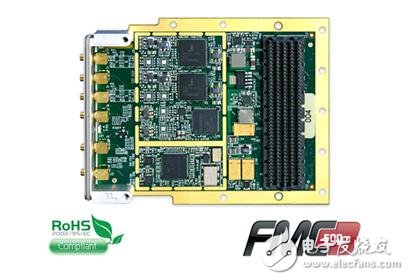
PEX6-COP is a flexible FPGA coprocessor card. It is an industry-standard, half-length PCIe desktop or server card with FMC input-output modules and integrated cores for Virtex6 FPGA computing.
The FPGA operating core uses the highest density LX550 and SX475 from Xilinx's Virtex6 FPGA family. The SX475 offers over 2000 DSP MAC elements operating at frequencies up to 500 MHz. The FPGA core has two banks of QDRII+ SRAM banks and three 512 MB DDR3 DRAMs. Each memory is completely independent and directly connected to the FPGA.
For system communication, the PEX6-COP has a PCIe and an auxiliary x4 port. The PCIe port is an x8 second-generation interface that supports sustained operations up to 2.5 GB/s and burst rates of 4 GB/s. Auxiliary ports can be used as Aurora ports (x4 to X1), as a second PCI Express x4 port, or using a custom protocol.
Meets VITA 57's FMC interface and provides PEX6-COP configurable input and output. The FMC interface fully supports high pin-count connectors, with more than 80 pairs of LVDSs directly connected to the FPGA and up to 5 Gbps per channel for 10 channels. FMC also easily adapts to application-specific custom modules.
The typical operation of the PEX-COP series power is less than 15W. The card can be adapted to the temperature range (-40°C to +85°C) and has a humidity of 100%.
The FPGA logic can be fully customized using the FrameWork logic's toolset. This tool provides support for MATLAB and RTL designs. The MATLAB BSP supports online development of the real-time hardware of the generator using the graphical block diagram Simulink environment and Xilinx System Generator. Applications such as DDC, demodulation and FFT signal processing cores for wireless communications, radar and signal intelligence applications are also available.
Host development software tools include C++ libraries and drivers for Windows and Linux (including real-time variants). And application examples showing the function of the module
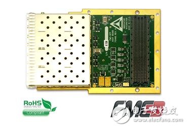
FMC high speed data acquisition and software radio interface board
FMC interface card with PEX6-COP; FMC-500M high-speed digital sum signal generation FMC IO module with support for two 500 MSPS A/D channels and two 500 MSPS D/A channels with sampling clock and trigger function .
The FMC-500M provides two 14-bit 500 MSPS 16-bit 250 MSPS A/D conversions, either AC or DC coupled, plus two 500 MSPS update rate DACs. The DAC can use a single 1 GHz output channel. Analog IO is AC or DC coupled. receiver? ? Supports up to 250 MHz IF frequency. The sampling clock is from a low jitter PLL or external input. Doka can be sampled synchronously.
The FMC-500M consumes 6W typical operation. The module is conductively cooled by the VITA20 standard and heat sink. Enhanced wide operating temperature from -40 to +85°C operation and vibration levels at 0.1 G2/Hz. Conformal coatings are available.
Support for VHDL logic is provided with the FPGA carrier card. Specific support content for InnovaTIve integraTIon carrier cards includes FrameWork logic tools and MATLAB development that support VHDL/Verilog. Carrier Card Integration for FMC Modules and FPGAs Matlab's Board Support Package supports Simulink environments using graphical block diagrams and online development of Xilinx System Generator real-time hardware.
The FMC-SFP+ provides four SFP+ ports in a standard FMC module with programmable clock and support functions. Fibre optics are connected to remote IOs, such as remote radio applications, and host processors and FPGA cards support bit rates up to 5 Gbps.
The SFP+ port is compatible with the SFF-XXXX transceiver and supports copper and fiber connections. The four-port module is completely independent. The SFP+ monitoring and control signals map to the FMC interface for detection, loss of signal, rate control, and I2C control ports.
A flexible reference clock on the FMC-SFP+ is fully programmable from 0.16 - 350 MHz. The clock can be programmed for all standard universal rate rates such as OC-12, CPRI, OBSAI, Gigabit Ethernet, sFPDP, and SONET. The maximum clock jitter is less than 1 ps RMS, making it able to meet the most stringent requirements of these applications. One card on the PLL reference is 10 MHz with 0.5 PPM stability.
The FMC-SFP+ is fully electrically compatible with the FMC (ANSI / VITA 57) specification IO modules. Physically, the module will conform to the FMC interface size but will protrude from the SFP on the faceplate. This module is compatible with 4 FMC HPC SFP ports or LPC (1 SFP port). When the SFP+ module is not included, the module consumes less than 500 milliwatts.
Interface VHDL code provided by FMC. Specific FPGA and platform support provides InnovaTIve IntegraTIon's VPX-COP and PEX-COP FPGA cards.
Relay Control Voltage Regulator
PC-TM series Relay Control Voltage Stabilizer has the low energy consumption,the over voltage protection,the low voltage protection,the over-current protection,the over-loading protection,the over-temperature protection and so on.It boasts for many kinds of protections,the collection energy conservation and the environmental protection ect.This is a brand-new concept product which possess many new technologies!This series products simultaneously ha applied for many technical monopolies
We already applied many kinds of this products patent, and the technical patent NO: 200720036394.1 and Appearance paten NO: 200730025909.3
2. Use for equipment:
Computer
Test equipment
Light system
Safe alarm system
Ray equipment
Medical equipment
Copy machine
Stereo equipment
Numerical control machine tools
Industrial automation equipment
Color and drying equipment
Test equipment
Hi-Fi equipment


Relay Control Voltage Regulator ,Voltage Regulator For Ac,3000Va Voltage Regulator,Wall Mount Voltage Stabilzier
zhejiang ttn electric co.,ltd , https://www.ttnpower.com