The Substrate Integrated Waveguide (SIW) is a new high-Q, low-loss integrated waveguide structure that is easy to design and process, and easy to integrate on a flat-panel circuit. It is low-cost and can be widely used in microwave and millimeter-wave integrated circuits. [1-4]. Due to the similarity with traditional rectangular waveguides, many design concepts can be borrowed, such as waveguide splitters, filters, antennas, and so on. In this paper, we use the wide-edge slitting of this guided wave structure to realize the directional coupler, and this paper adopts the semi-membrane structure, which can reduce the size of nearly half but does not affect its performance. Finally, the simulation results are also consistent. Theoretical analysis and research have achieved the intended purpose.
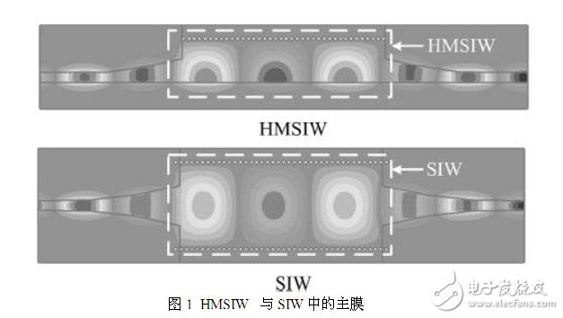
When the substrate integrated waveguide operates in the main mode, the field value of the electric field reaches a maximum value and the value of the magnetic field is almost zero in the waveguide symmetry plane along the wave propagation direction, so the symmetry plane can be equivalent to a magnetic wall. Thus, the substrate integrated waveguide can be divided into two halves by an imaginary magnetic wall, and each half becomes a substrate integrated waveguide of a half-membrane structure, and the energy is almost entirely bound inside, and the energy leaked from the split surface is neglected. Figure 1 shows the comparison of the main film in HMSW and SIW.
In this paper, the HMSIW directional coupler we studied is mainly inspired by the waveguide directional coupler. Using the waveguide wide-side slot coupling theory, an elongated slot is opened at the appropriate position on the common wide wall of the two waveguides for energy coupling. A new structure of SIW directional coupler. Since we are using a substrate-integrated waveguide, we need to overlap the ground planes of the two SIWs so that the upper and lower SIWs can be seen as two waveguides with a common wide wall, so the gap is opened in the middle of the structure. The layer ground plate decouples energy, which is equivalent to the wide-side slit waveguide coupling. Since it is a semi-membrane structure, it is necessary to consider the position of the gap. Through simulation analysis and research, the coupling of the position of the slit in the vicinity of the metallized hole is better. Figure 2 shows the designed HMSW directional coupler structure, specifically indicating that the gap is the ground layer in the middle, not on the upper and lower microstrips.
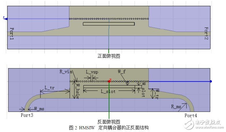
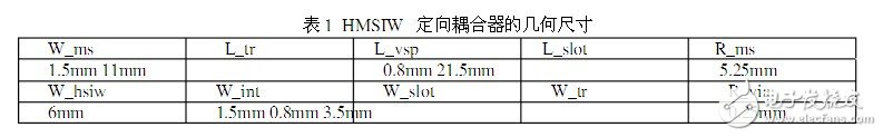
We must consider the size of the SIW directional coupler (5-6) according to its design principle. For HMSW directional couplers operating in the same frequency band, the width (W_hsiw) can be set to half of the SIW directional coupler, HMSIW to microstrip The transition line width (W_tr) of the line is also about half of the transition line from the SIW to the microstrip line. The transition setting between the SIW and the microstrip can be referred to (7-8). The initial value of the position and size of the coupling gap can be set according to the waveguide theory working in the same frequency band, and then optimized and finally reached the optimal value. Table 1 is the geometry of the HMSIW directional coupler we designed. The coupling gap length is set according to a 3dB directional coupler. Of course, the amount of coupling can be changed by changing the value of the slot length.
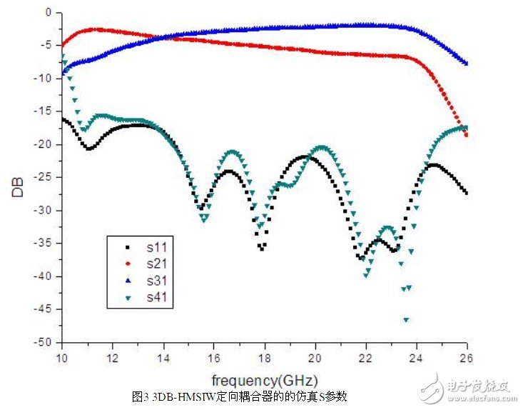
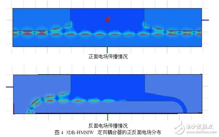
The coupler operates in the range of 14 GHz to 24 GHz. The thickness of the selected dielectric substrate is h = 0.5 mm, the dielectric constant is 2.2 r ε = , the tangent tangent tan δ = 0.0009, and the conduction band thickness t = 0.035 mm. The 3D full-wave electromagnetic simulation software HFSS is used to simulate and optimize the HMSW directional coupler to achieve the best results. The results of the simulated S-parameters corresponding to Table 1 are shown in Fig. 3. At this time, the corresponding electric field distribution in the substrate integrated waveguide is shown in Fig. 4. We can see that energy is coupled from the 1 port of the main waveguide to the sub-waveguide through the slot. The 3 ports have no obvious energy leaks.
This paper proposes a new structure of an ideal HMSIW directional coupler. Its main features are small size, large isolation, low loss and wide bandwidth, which have crossed the KU and K bands. Can be used in highly integrated microwave circuits and millimeter wave circuits. The substrate integrated waveguide directional coupler has great flexibility in design, not only simple processing, low cost, but also can directly borrow some concepts and design methods of the traditional waveguide, so that it can be fully realized.
Uv Curing Hydrogel Film,Glass Protector,Matte Frosted Antiglare Full Cover Screen Protector,Cut Screen Protector Glass
Shenzhen TUOLI Electronic Technology Co., Ltd. , https://www.hydrogelprotector.com