2. Hubei Province Power Grid Intelligent Control and Equipment Engineering Technology Research Center, Wuhan 430068, China)
Abstract: PC104 bus is an industrial control line defined for embedded control systems. It has a wide range of applications, but its internal structure is complex and it is difficult to detect faults. An FPGA-based PC104 bus fault automatic monitoring platform is designed to perform real-time monitoring and fault detection on the PC104 bus signal. The platform uses the FPGA program to collect and process bus signals, and transmits them to the host computer for processing and display. The system uses the FPGA program to implement its functional modules, including capturing the POST power-on self-test command and BIOS self-test port code, monitoring the bus voltage level, monitoring the quality of key signals such as clock and reset, controlling the PC104's automatic reset and BIOS setup mode, etc. Features. The monitoring results obtained by the host computer and the real-time detection of the FPGA are given, which reflects the technical requirements of the FPGA program to meet the PC104 bus detection in this system.
Keywords: bus monitoring; POST power-on self-test; self-test port monitoring; clock measurement
CLC number: TN407; TP206
Document identification code: A
DOI: 10.16157/j.issn.0258-7998.170644
Chinese citation format: Zhou Zhihu, Zhang Fan, Wu Minghu, et al. FPGA programming for PC104 fault monitoring platform [J]. Electronic Technology Application, 2017, 43(9): 57-60.
English reference format: Zhou Zhihu, Zhang Fan, Wu Minghu, et al. FPGA program design of PC104 fault monitoring platform[J].Application of Electronic Technique,2017,43(9):57-60.
0 Preface
As a special embedded control board [1], PC104 has the advantages of low power consumption, high efficiency, small size, and expandability. It is used in aerospace [2], military weapons and equipment [3], industrial control [4] and other fields. Wide range of applications. The structure of the PC104 motherboard is complex and compact. Once a fault occurs, it is difficult to determine the specific cause of the fault by conventional monitoring means. The PC104 bus needs to monitor up to 70 signals, and the bus running frequency is also up to 14 MHz. It is impossible to use the single-chip microcomputer to realize the monitoring function [5-6]. Therefore, this project adopts an FPGA-based design scheme, which uses the multi-I/O port characteristics of the FPGA and high-speed parallel processing capability [7] to monitor the PC104 bus in real time.
1 PC104 monitoring system design
The FPGA-based PC104 fault monitoring platform (hereinafter referred to as the monitoring platform) is mainly composed of the PC104 motherboard, the level signal conversion module, the FPGA function module (DE0 development board) [9], and the host computer system. The hardware structure of the monitoring platform is shown in Figure 1.

The upper computer system board in the monitoring platform uses the common Windows XP system and automatically runs the monitoring APP program. Through the serial port and the FPGA function module communication, the information returned by the FPGA function module is read by using the agreed communication protocol, and the returned information is processed into reference data, and finally displayed in the interface of the upper computer APP program.
The PC104 motherboard is powerful and has a lot of extended function ports. In order to judge its specific fault information, the monitoring platform needs to monitor its bus signal in real time. In order to ensure the convenient and efficient operation of the monitoring platform, the motherboard fixture is introduced under the test to facilitate the plugging and unplugging of the motherboard, which not only improves the monitoring efficiency and accuracy, but also protects the PC104 motherboard bus interface from being damaged.
Since the PC104 motherboard works in a +5 V power supply environment and the operating voltage of the FPGA is +3.3 V, the monitoring platform incorporates a level signal conversion module based on the 74AL-VC164245. The 74ALVC164245 is a level-shifting chip that is manufactured by TI and is bidirectionally converted between +5 V and +3.3 V. It can achieve level matching between FPGA and PC104 motherboard. The adapter board also includes the PC104 motherboard power supply test module, and expands the keyboard interface, mouse interface and two serial ports on the PC104 motherboard. Not only real-time transmission of signals between different levels is realized, but also the space utilization of the monitoring platform is increased.
2 FPGA function module design
The FPGA function module is the core of the PC104 motherboard fault detection platform and is the focus of this article. FPGA has programmable input and output unit (IOB), configurable logic block (CLB), digital clock management module (DCM), embedded block RAM (BRAM), rich routing resources and other functions, which can well meet the detection platform. Related needs. Not only can the PC104 bus signal be acquired in real time, but also the operating state of the PC104 motherboard can be controlled by controlling the relevant pins on the bus by outputting TTL level signals. The use of FPGA functional modules as the core of the detection platform greatly improves the reliability and efficiency of the detection platform.
2.1 BIOS boot monitoring and POST power-on self-test
The off-chip bus interface of the PC104 main board includes its address signal line, latched address signal line, and data signal line, including 20 address signal lines and 16 data signal lines. The basic principle of the monitoring platform to achieve this function is to monitor the status of all signal signal lines and data signal lines when the PC104 main board is started by the signal acquisition port of the FPGA to determine whether the working status of each signal line is normal. The specific FPGA program design flow chart for realizing the bus signal monitoring function is shown in Figure 2.
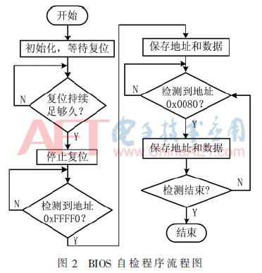
2.1.1 BIOS boot detection
The startup process of the PC104 motherboard includes power-up, bootstrap, core test, and POST self-test. After the monitoring platform is powered on, the test is started. After the PC104 main board is powered on, a reset command is issued to the motherboard. After the main board enters the initialization process and the reset duration is satisfied, the reset signal is released. The address line monitoring port of the FPGA starts to read the data of the address signal line. If the read address line data is 0xFFFF0H, the program for monitoring the startup code of the PC104 motherboard is started, and the address and data on the bus are saved.
From the PC104 motherboard user manual, it is known that when it starts up, it usually runs an "EA" jump instruction and jumps to the start address of the actual BIOS ROM. The process of initializing the search address 0xFFFF0H and subsequent CPU redirection is generally referred to as bootstrapping or booting, and may also be referred to as BOOT for short. When the PC104 starts up, the address and data line signals on the FPGA acquisition bus will ideally jump to a fixed address unit via the jump instruction "EA" and start executing the program. Monitor the actual measured data of the BIOS startup code of the two normal running boards, as shown in Table 1.
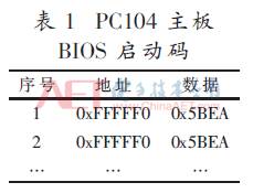
It can be seen from the data in the table that when the motherboard starts normally, the program starts from 0xFFFFF0 address, and the first instruction executed is 0x5BEA, according to which it can be judged that the data and address bus of the motherboard is not faulty. The monitoring results meet the test requirements.
2.1.2 POST power-on self-test
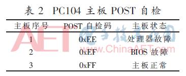
PC104 motherboard initialization is divided into cold start (initial power-on start) and hot start (restart by FPGA to send reset command). If it is cold start, POST power-on self-test will be performed; otherwise, POST power-on self-test will be skipped. When an error is encountered, the single-byte POST code is written to the 80H I/O port and the system initialization is terminated. If the self-test passes, it will return 0xFF to the 80H I/O port. The self-test process of the motherboard is a standard for judging whether the PC104 motherboard is normal, so the POST self-test is one of the most important modules for judging the fault information of the motherboard. When the FPGA monitors the startup of the PC104 motherboard, it starts to periodically read the signals in the 80H I/O port. When 0xFF is read, the signal is saved and returned to the host computer system, prompting the self-test to pass; otherwise, the fault command is returned and the self-test fails. By comparing the POST monitoring results of three different PC104 motherboards, and referring to the actual operating state of the motherboard, it can be seen that the test requirements are met. During the test, if the motherboard just starts the POST self-test code and monitors 0xFF, and the start code does not change, it may be that the motherboard is not running. The BIOS self-test does not start normally. The PC104 motherboard should be restarted and retested. . The POST power-on self-test results are shown in Table 2.
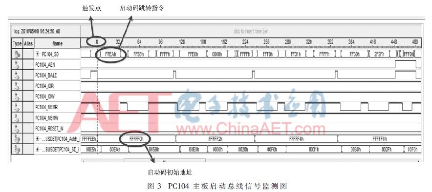
Using FPGA to collect the results of bus detection during startup of PC104 motherboard, as shown in Figure 3. From the figure, it can be seen intuitively that the initialization process and POST self-test results included in the startup process of the PC104 motherboard meet the bus test requirements.
2.2 PC104 reset and BIOS mode control
During the operation of the monitoring platform, it is required to perform repeated tests on the same PC104 motherboard. Due to the high integration of the PC104 motherboard, there is no reset button, so you need to control the reset switch (Reset Switch) pin on the motherboard for reset control. When the host computer system issues a reset command, the FPGA needs to send a delay reset command to the reset control pin of the PC104 motherboard, and monitor the start timer. When the reset time arrives, the reset signal is released.
The system expansion module uses the floppy disk drive controller manufactured by Shengbo Technology to meet the PC104 bus standard to drive the hard disk with the test program. The test program can monitor the fault information of the serial port and keyboard interface of the PC104 motherboard. In order to set the basic hardware information such as the startup mode of the PC014 motherboard and the status and resolution of the display, it is necessary to control whether it enters the BIOS at startup. The basic control circuit consisting of a relay and a triode is controlled by the I/O port of the FPGA to control whether the DTR and RI pins of the serial port connector of the main board are short-circuited to control whether the BIOS setting is entered during startup.
2.3 PC104 key signal measurement
There are four key signals in the PC104 main board bus control signal line, including three clock signals and one reset pulse signal.
2.3.1 PC104 bus clock frequency measurement
The commonly used methods for measuring frequency of FPGA include direct frequency measurement method and equal precision frequency measurement method. The direct frequency measurement method is further divided into direct counting frequency measurement method and measurement period frequency measurement method. The frequency measurement accuracy of the direct frequency measurement method is related to the measured signal. The higher the frequency of the measured signal, the higher the frequency measurement accuracy; the implementation is simple, and the hardware resources are not required. The accuracy of the frequency measurement method of the equal-precision frequency measurement method is independent of the signal to be measured. It is only related to the system clock signal. The higher the frequency of the system clock signal, the higher the accuracy. Compared with the direct frequency measurement method, the accuracy measurement method is more complicated and needs to be realized. The crystal frequency of the FPGA system meets the frequency measurement accuracy requirements of equal precision frequency measurement.
The clock signals to be tested are: REFRESH# The memory refresh signal line is driven by the refresh controller to indicate that a refresh cycle will be executed; BCLK is the system bus clock signal line driven by the platform circuit, and the frequency is 6 MHz under normal operating conditions. 8 MHz (±500 ppm), the duty cycle of the cycle is 45% to 55%; the OSC oscillator signal line is the clock signal driven by the platform circuit, the frequency is 14.318 18 MHz (±500 ppm), the duty of the cycle The ratio is 45% to 55%. The OSC is not synchronized with any other bus signal lines. The minimum frequency to be tested is 6 MHz. The direct counting frequency measurement method can be used. The measurement accuracy can reach 10-6 and 10-7 respectively, which meets the technical requirements for measuring 1% error of this frequency. The direct counting frequency measurement method is simple in implementation, small in calculation amount, and improves the running speed of the monitoring platform.
2.3.2 PC104 bus reset pulse width measurement
The pulse width test measures the pulse width of the reset pulse during the reset of the PC104 motherboard, and the reset signal line is driven to the active state by the platform circuit. Any bus resources that receive a reset signal must immediately tri-state all output drivers and enter the appropriate reset state.
The pulse width of the FPGA is usually measured by the pulse counting method, that is, the high level or the low level of the signal to be tested is counted by a high frequency clock pulse, and then the width of the signal to be tested is calculated according to the number of pulses. The signal to be tested is usually independent of the count clock, and its rising and falling edges cannot fall exactly on the edge of the clock, so the maximum measurement error of the method is one clock cycle. The monitoring platform FPGA adopts a 50 MHz high-frequency clock, and the pulse width measurement accuracy can reach 2×10⁻⁸, which satisfies the technical requirements of PC104 motherboard monitoring reset pulse width measurement.
2.4 Power Measurement Module
The voltage monitoring module is based on the AD7417 from Analog Devices, Inc. The AD7417 is a tens, four-channel analog-to-digital converter with on-chip temperature sensors. The AD7417 has exceptional performance in reducing power consumption. Its automatic power-down feature allows the chip to initiate a power-down mode at a lower output rate to reduce power consumption.
The working voltage of the PC104 motherboard is +5 V, and the operating voltage of some modules is +12 V. The AD7417 has four AD conversion channels that can be monitored for ±5 V and ±12 V of the bus. Using the I/O port of the FPGA and the SDA and SCL of the AD7417 to form a two-wire I2C serial bus interface, the AD7417 chip is controlled by the FPGA to collect the respective power supply voltages on the PC104 bus, and the collected results are AD-converted and uploaded to FPGA processing.
The voltage test module input circuit schematic is shown in Figure 4. The positive voltage of the bus adopts the series voltage division of the resistor to obtain the analog voltage value that can be recognized by the AD7417; the negative voltage of the bus passes through the reverse voltage regulator diode of 8.2 V to obtain a positive voltage, and then the voltage is divided into identifiable voltage values. The following takes the +5 V test input port as an example to introduce the actual voltage value calculation method.

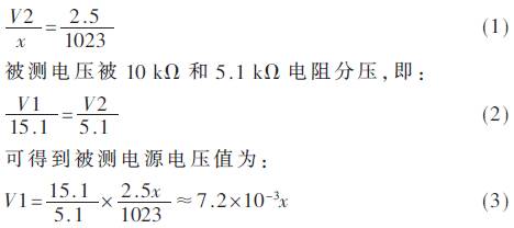
It is known that the reference voltage of the AD7417 is an internal reference voltage of 2.5 V. Assuming that the actual measured voltage is V1, the input voltage of the AD7417 input port IN1 is V2, and the value collected by the FPGA is x, then:
3 Conclusion
The FPGA monitoring program designed by this project can not only effectively record the bus running code of PC104, but also extract the effective starting code and fault monitoring code in real time, and measure the frequency and pulse width of the key signals of the bus. The FPGA program communicates with the host computer in real time, and can realize functions such as information uploading, reset control, and BIOS mode control according to the instructions of the host computer. The design has been tested several times to effectively detect the faulty PC104 motherboard and provide specific fault information. It can be seen from the test results that the detection program based on FPGA design can meet the detection technical requirements of PC104 motherboard system in both speed and function. The system of the design is convenient to operate, has strong expandability and good practicability. At present, the PC104 monitoring platform using the FPGA program meets the technical requirements and passes the acceptance.
references
[1] Liu Guanglin. Design and application of industrial control platform based on PC/104 and ARM [D]. Wuhan: Huazhong University of Science and Technology, 2010.
[2] Yang Yongzhi, Huang Shenglun, Feng Hejun, et al. ATS of a certain aircraft weapon control system based on PC/104 bus[J]. Journal of Air Force Engineering University (Natural Science Edition), 2003, 4(3): 36-39.
[3] Zhang Zhonghua, Gao Xiaozhuang, Wang Dapeng. Detection and Maintenance Platform of Radar Master Control Unit Based on PC104[J].现代电å技术,2015,38(3):48-50.
[4] Chen Fang. Design and implementation of ARINC 429 communication bus based on PC/104 [D]. Nanjing: Nanjing University of Aeronautics and Astronautics, 2005.
[5] Chen Zhengjie, He Jian. Design of Embedded Computer Motherboard Detection Card Based on CPLD and PC104 Bus Specification[J].Measurement & Control Technology,2006,2(25):331-336.
[6] Chen Yanshen, Zhang Bo, Guan Shaohui, et al. PCI04 Motherboard Detection System Based on OMAPLl38 and FPGA Architecture[J]. Computer Measurement & Control, 2015, 23(5): 1512-1514.
[7] Yang Haigang, Sun Jiabin, Wang Wei. A Review of the Development of FPGA Device Design Technology[J].Journal of Electronics & Information Technology,2010,32(3):714-727.
[8] Zhang Yuming, Li Qi, Li Jinhai, et al. Design of portable GNSS signal acquisition and playback system based on ARM and FPGA[J].Application of Electronic Technique, 2016, 42(10): 58-61.
[9] Altera Corporation, Terasic Technologies. DE0 user manual [EB/OL]. (2011) [2017]http://DE0.terasic.com.


Bitcoin mining is the process of creating new bitcoin by solving puzzles. It consists of computing systems equipped with specialized chips competing to solve mathematical puzzles. The first bitcoin miner (as these systems are called) to solve the puzzle is rewarded with bitcoin. The mining process also confirms transactions on the cryptocurrency's network and makes them trustworthy.
For a short time after Bitcoin was launched, it was mined on desktop computers with regular central processing units (CPUs). But the process was extremely slow. Now the cryptocurrency is generated using large mining pools spread across many geographies. Bitcoin miners aggregate mining systems that consume massive amounts of electricity to mine the cryptocurrency.In regions where electricity is generated using fossil fuels, bitcoin mining is considered detrimental to the environment. As a result, many bitcoin miners have moved operations to places with renewable sources of energy to reduce Bitcoin's impact on climate change.
Btc Miner,Bitmain S19 Xp,Bitmain Antminer S19 Xp,Antminer Bitmain S19 Xp 140Th
Shenzhen YLHM Technology Co., Ltd. , https://www.asicminer-ylhm.com