Optocouplers seem to be able to achieve simple DC isolation between circuits operating at different ground potentials, but this is only a surface phenomenon. The optocoupler draws power from the isolated circuit, which is relatively slow to convert and has the uncertainty of LED aging. There are now some alternatives that do not require optocouplers, such as Analog Devices' ADUM12xx or Texas Instruments' ISO72x. This design example will describe a simple and improved method of optocoupler.
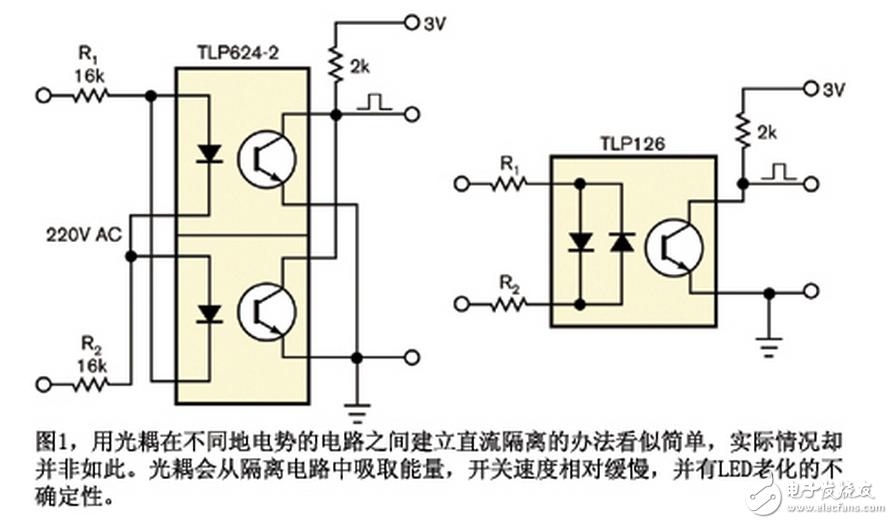
Figure 1 shows two common 0 V AC synchronous designs. It attempts to reduce the LED current of the optocoupler by increasing the load resistance of the optocoupler accordingly, thereby reducing the power consumption of the isolation circuit, but the result is a slower and more uncertain switching speed. In order to achieve a faster and simpler switch, power efficiency must be sacrificed; however, the advantages of this sacrifice are limited because the power supply efficiency is inversely related to the AC voltage strength.
For example, optocouplers continuously emit more than the nominal value in almost all AC cycles, resulting in low power efficiency and relatively fast aging of the optocoupler. A larger disadvantage is the excessive and almost uncontrollable zero-crossing distortion because the sensitivity threshold of the circuit depends on the parameters of the optocoupler. The design in Figure 1 does not provide an ideal Solution. As for the efficiency, according to the current transfer ratio of the optocoupler and the AC amplitude, the current drawn by them is 5 mA to 100 mA.
The design in Figure 2 solves the problem of excessive power consumption, uncertain switching and LED aging, making it ideal for wide AC range applications. Compared with the circuit in Figure 1, the LE of Figure 2
D only illuminates when it is close to the zero crossing point, and derives energy from the previously charged capacitor, thus reducing the average current by one tenth to one hundredth. The design also provides faster, more deterministic and steeper conversions. In addition, the expected LED aging problem is also slowed down. The heat dissipation of resistors R1 and R2 in Figure 1 is less than 1.5 W, so replacing them with 0.1 W devices allows more components to be placed on the same board area (Figure 2).
The main components of the circuit include amplitude detector D1, capacitor C1 and Schmitt trigger Q1/Q2 for controlling the current through the optocoupler LED. D2 and D3 are used to stabilize the base voltage of Q2 while also stabilizing the collector current of the starting optocoupler. Capacitor C1 is charged through R1, R2, and D1.
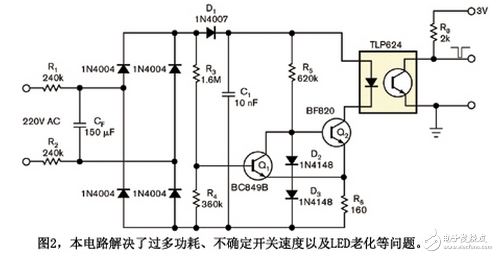
In almost all AC cycles, except for the near zero crossing point, Q1 is on and Q2 is off. Therefore, near the zero crossing point, the state of the Schmitt triggers Q1 and Q2 is reversed, and Q2 causes the capacitor C1 to discharge at a constant current because the circuit composed of Q2, D2, D3, R5, and R6 stabilizes the current at I = ( 2 &TImes; VD - VBE2) / R6, where VD is the voltage drop across D2 or D3, and VBE2 is the base shot voltage of Q2.
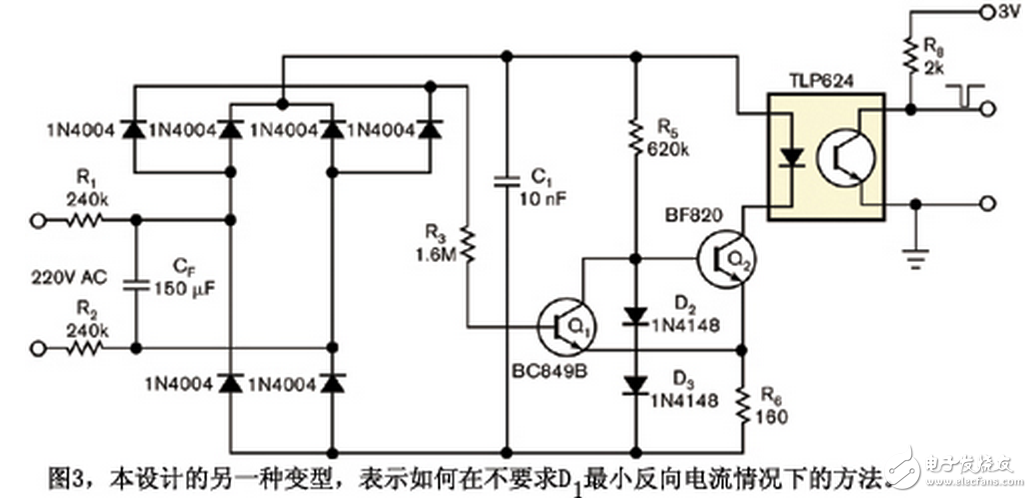
Schmitt triggers have a natural hysteresis effect, while some applications do not require this hysteresis. Figure 3 is such a design. It also shows the method when D1 minimum reverse current is not required. But this circuit is best suited for purely synchronous and non-triac controlled. Due to the stability of the LED current, these designs extend the AC input voltage range and may be useful for a variety of AC powered small products; and are a set LED current without the risk of LED overload; and also reduce the optocoupler The impact of stability. A further advantage of these designs is that they are inherently safer. In the event of a short circuit in the terminal, the current between the isolated and non-isolated sides can be one-tenth to one-hundredth less than the circuit of Figure 1. Optocouplers also have advantages. Due to the low duty cycle, the value of the optocoupler load resistor R8 can be freely reduced without loss of power efficiency. This reduction results in a low zero crossing error.
What are the future LED packaging formats going to be developed?1. Medium power has become the mainstream packaging method. At present, most of the products on the market are high-power LED products or low-power LED products. Although they have their own advantages, they also have insurmountable defects. The medium-power LED products that combine the advantages of both have emerged as the mainstream packaging method.
2. The application of new materials in packaging. Materials such as thermoset materials EMC, thermoplastic PCT, modified PPA, and ceramic-like plastics will be widely used due to higher and better environmental tolerances such as high temperature resistance, UV resistance, and low water absorption.
3. Chip super current density application. In the future, the chip's ultra-current density will grow from 350MA/mm2 to 700MA/mm2 or even higher. The chip demand voltage will be lower, a smoother VI curve (lower heat), and ESD and VF.
4. Popularization of COB applications. With the advantages of low thermal resistance, good light quality, solder-free and low cost, COM applications will be widely used in the future.
5. The demand for higher light quality. Mainly for indoor lighting, Jingtai Optoelectronics will use the LED indoor lighting product RA to reach 80 as the standard, and RA to achieve the goal of 90. Try to make the light color of the lighting product close to the Plank curve, so that the light can be even and glare-free. .
6. International and domestic standards are further improved. It is believed that with the continuous improvement of LED packaging technology, the quality standards for LED products in China and internationally will continue to improve.
7. Integrated packaged light engine becomes the package value. The integrated packaged light engine will become the focus of the next season of the company.
8, go to the power solution (high voltage LED). In the future, indoor lighting will pay more attention to quality, and driven by cost factors, the power supply scheme will gradually become an acceptable product, and the high-voltage LED fully caters to the power-off scheme, but the need to solve the problem is that the chip reliability needs to be strengthened.
9. Multi-color LED light source for scene lighting. Scenario lighting will be the core competitiveness of LED lighting, and the second take-off of future LED lighting needs to rely on scene lighting to achieve.
10, the light efficiency demand is relatively reduced, cost-effective has become a magic weapon for the packaging factory. In the future, indoor lighting will not pay too much attention to light efficiency, but will pay more attention to the quality of light. With the improvement of packaging technology, the cost of LED lamps has become a power to replace traditional lighting sources. In the process of entering home lighting, the price/performance ratio will be more and more valued by customers.
Charging Pile Energy Management Solution
Charging Pile Energy Management Solution,Charging Pile DC Energy Meter,Charging Pile AC Energy Meter,Bidirectional DC Energy Meter,Electric Car Charging Pile Energy Meter
Jiangsu Acrel Electrical Manufacturing Co., LTD. , https://www.acrel.com.pk