Summary of content: TPS5430 is a DC/DC switching power conversion chip newly launched by TI (Texas Instruments). Its superior performance has caused it to receive widespread attention as soon as it went on the market. This article describes the characteristics, parameters, functions, and structure of the chip, and introduces its application in seismic precursor observation instruments in combination with practical conditions.
I. Introduction
Earthquake precursor observation instrument is an important part of earthquake precursor observation. Only when the instrument is stable and reliable can it provide continuous raw data for earthquake precursor analysis. Continuous excavation and the use of high-performance components to replace relatively low-performance, old components is a way to improve the performance of the instrument.
TPS5430 is a DC/DC switching power conversion chip with superior performance newly launched by TI. We developed it and applied it to the data acquisition system of the TJ-2 volumetric strain gauge.
2. Introduction to TPS5430
1. TPS5430 features
TPS5430 has good characteristics, its performance and main parameters are as follows:
High current output: 3A (peak 4A);
Wide voltage input range: 5.5~36V;
High conversion efficiency: up to 95% in the best condition;
Wide voltage output range: the minimum can be adjusted down to 1.221V;
Internal compensation minimizes the number of external components;
Fixed 500kHz conversion rate;
With overcurrent protection and thermal shutdown function;
With switch enable pin, only 17uA quiescent current in off state;
Compared with other DC switching power conversion chips of the same type, the high conversion efficiency of TPS5430 is particularly worthy of attention.
Figure 1 is a graph showing the relationship between TPS5430 conversion efficiency and output current at 12V input voltage and 5V output voltage.
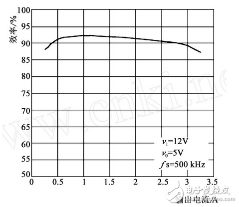
Figure 1 TPS5430 chip efficiency-current relationship curve
2. Function and structure
(1) Pin description:
TPS5430 adopts 8-pin SO IC PowerPADTM package, as shown in Figure 2.
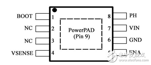
Figure 2 TPS5430 package
(2) Internal structure and function:
â‘ Oscillator frequency.
The 500kHz conversion rate is fixed, so that a smaller output inductance can be produced under the same output ripple requirement.
â‘¡ Reference (Reference) voltage.
By scaling the output range of the temperature-stabilized band gap circuit, the reference voltage system generates an accurate reference signal. After testing, within the allowable temperature range, the band gap and the scaling circuit remain balanced when the voltage is output at 1.221V.
â‘¢ ENA (enable pin) and (Slow Start) internal soft start.
When the voltage on the ENA pin exceeds the limit voltage, the converter and the internal soft start will start to work. When the voltage on the ENA pin is lower than the limit voltage, the converter will stop working and the soft start will start to reset. The converter stops working when the ENA pin is grounded or the voltage is less than 015V. ENA pin can be left floating.
â‘£ UVLO (under voltage lockout).
TPS5430 has UVLO circuit. No matter in the process of power-on or power-down, as long as V IN (input voltage) is lower than the limit voltage, the conversion chip does not work. The typical hysteresis of the UVLO comparator is 330mV.
⑤ Boost CaPACitor (starting capacitor).
Connect a 0.01μF ceramic capacitor between the BOOT pin and the PH pin to provide the gate voltage for the high side of the MOSFET.
â‘¥ VSENSE (external feedback) and Internal CompensaTIon (internal compensation).
The output voltage is fed back to the VSENSE pin through an external resistor divider. In the steady state, the voltage of the VSENSE pin is equal to the voltage reference value of 1.221V. The TPS5430 has an internal compensation circuit, which simplifies the chip design.
⑦ Voltage Feed Forward (voltage positive feedback).
The internal voltage positive feedback ensures that the power chip has a constant gain no matter how the input voltage changes. This greatly simplifies stability analysis and improves transient response. The positive feedback gain of TPS5430 is typically 25.
⑧ Pulse-W idth-ModulaTIon Control (pulse width control).
The converter adopts a fixed frequency control method.
⑨ Overcurrent Protection.
When the overcurrent protection circuit makes the current exceed the limit value, the internal overcurrent indicator is set to true, and the overcurrent protection is triggered.
â‘© Thermal Shutdown.
When the junction temperature exceeds the temperature cut-off point, the voltage parameter is set to ground, and the high-side MOSFET is turned off. Under the control of the soft-start circuit, when the contact temperature drops to 14°C lower than the temperature cut-off point, the chip restarts.
3. The application of TPS5430 in the seismic precursor observation data acquisition system
The data acquisition system is an important part of the seismic precursor observation instrument. It converts the weak analog signal detected by the sensor into a digital signal and performs calculations to provide reliable data for subsequent seismic analysis.
Initially, we used a chip power supply such as MAX1626 to power the TJ-2 volumetric strain gauge data acquisition system, but in the test we found that the system was unstable and the instrument would automatically restart. Investigating the reason, it was found that the load capacity of chip power supplies such as MAX1626 was not large enough. Therefore, after many investigations, we finally chose the TPS5430 chip with strong load capacity, high efficiency and few peripheral components as the power supply to supply power for the A/D conversion module and data processing module of the data acquisition system. The principle is shown in Figure 3.

Figure 3 Schematic diagram of the data acquisition system.
1. Circuit design
In the process of designing the power supply for the TJ-2 volumetric strain gauge data acquisition system, first determine the design parameters according to the work requirements, and then design the circuit and select the peripheral components according to the parameters.
(1) Design parameter requirements
Input voltage range: 10.8~19.8V; output voltage: 5V; input ripple voltage: 300mV; output ripple voltage: 30mV; output rated current: 3A.
(2) Application circuit
The power supply design of this system selects the classic circuit of TPS5430, as shown in Figure 4.
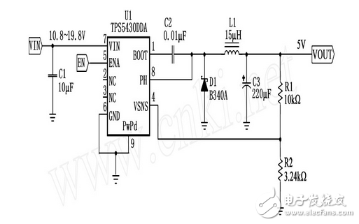
Figure 4 Application circuit diagram of 1018~1918V input to 5V output voltage
(3) Selection of components
â‘ Input capacitance.
TPS5430 requires a slightly larger decoupling capacitor. A high-performance ceramic capacitor of 10μF (C 1) is recommended here. You can also choose a smaller capacitor, but it must meet the input voltage and rated current ripple requirements.
â‘¡ Output filter components.
The output filter device, namely L 1, C 2. TPS5430 has an internal compensation circuit. The output inductance is related to the maximum output current, and 15μH inductance is selected here.
The output capacitance is an important design factor that affects the rated voltage, rated ripple current, and equivalent impedance (ESR). In this application, 220μF output capacitor is selected. At this time, the RMS ripple current generated in the circuit is 143mA, and the maximum ESR required is 40MΩ.
â‘¢Output voltage setting.
The output voltage is determined by the resistance (R 1, R 2) of the VSENSE pin. If the output voltage is 5.0V, the reference voltage is 1.221V, and R1 is 10kΩ, then R2 is determined to be 3.24kΩ.
â‘£ BOOT (start) capacitor.
Choose 0.01μF for BOOT capacitor C 2.
⑤ Capture diode.
TPS5430 needs an external capture diode, choose B340A, its reverse voltage is 40V, forward current is 3A, and forward voltage is 0.5V.
2. Circuit board design
TI Company recommends the circuit board wiring and component placement diagram of the 10.8~19.8V input to 5V output voltage of TPS5430, as shown in Figure 5.
The circuit board design process of TPS5430 should follow the design principles of general power conversion chip circuits to achieve the desired effect. There are two more points to note:
â‘ PowerPAD is required to be connected to the ground. A pad can be placed directly under the chip, and through holes can be drilled to facilitate correct Ma Aihong, etc.: Power conversion chip TPS5430 and its application welding.
â‘¡ When there is no special requirement for ENA pin, it can be left floating, or signal vias can be reserved.
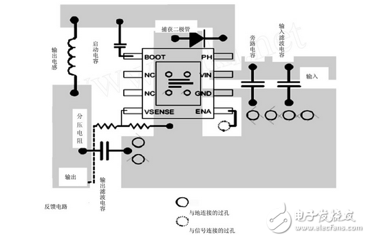
Figure 5 Circuit board design diagram
4. Conclusion.
At present, the data acquisition instrument of the TJ22 type volumetric strain gauge powered by the TPS5430 power supply has been practically used in many seismic stations in Inner Mongolia, Yunnan and so on. It has been verified that the power supply is in good working condition, all performances can meet the working requirements, and it can be extended to other hardware designs.
Dongguan Guancheng Precision Plastic Manufacturing Co., Ltd. , http://www.dpowerchargers.com