introduction
With the development of technology, mobile electronic devices have become an important part of our lives and culture. The application of tablet and smartphone touch technology allows us to interact more with these devices. It constitutes a complete electrostatic discharge (ESD) hazardous environment, that is, the electrostatic discharge of human skin to the device. For example, when using consumer electronics, ESD can occur between the user's finger and the tablet's USB or HDMI interface, causing irreversible damage to the tablet, such as peak standby current or permanent system failure.
This article will explain the differences between system-level ESD phenomena and device-level ESD phenomena and introduce you to some system-level design methods that provide ESD event protection.
System level ESD protection versus device level ESD protection
ESD damage to the IC can occur at any time, from assembly to board level soldering to end user human interaction. ESD-related damage dates back to the early days of semiconductor development, but it became a common problem in the 1970s when microchips and thin-gate oxide FETs were used in highly integrated ICs. All ICs have embedded device-level ESD structures that protect the IC from ESD events during the manufacturing phase. These events can be simulated by three different device-level models: Human Body Model (HBM), Machine Model (MM), and Charged Device Model (CDM). HBM is used to simulate ESD events caused by user operations, MM is used to simulate ESD events caused by automatic operations, and CDM is used to simulate ESD events caused by product charging/discharging. These models are used for testing in a manufacturing environment. In this environment, assembly, final testing, and board-level soldering are all done in a controlled ESD environment, reducing the ESD stress experienced by exposed devices. In a manufacturing environment, ICs can only withstand ESD shocks of 2-kV HBM, and the recently introduced small devices have electrostatic regulations as low as 500V.
Although device-level models are usually sufficient in a plant-controlled ESD environment, they are far behind in system-level testing. In an end-user environment, the ESD shock intensity of voltage and current is much higher. Therefore, the industrial environment uses another method for system level ESD testing, which is defined by the IEC 61000-4-2 standard. The purpose of device-level HBM, MM, and CDM testing is to ensure that the IC is not damaged during manufacturing; system-level tests specified in IEC 61000-4-2 are used to simulate end-user ESD events in the real world.
The IEC specifies two system level tests: contact discharge and non-contact discharge. When using the contact discharge method, the test simulator electrode is in contact with the device under test (DUT). In the case of non-contact discharge, the charged electrode of the simulator is close to the DUT, and a spark generated between the DUT and the DUT causes discharge.
Table 1 lists the test level ranges for each of the methods specified in the IEC 61000-4-2 standard. Please note that the discharge intensity is not the same for each test level of the two methods. We usually test the stress levels step by step above level 4 (the highest official nominal level for each method) until the point of failure occurs.

Table 1 Test levels for contact discharge and non-contact discharge methods
There are some significant differences between device-level and system-level models, and Table 2 lists these differences. The last three parameters in Table 2 (current, rise time, and number of shocks) require special attention:
• Current difference is critical for ESD-sensitive devices to withstand an ESD event. The 8-kV HBM protection chip (peak current 5.33A) may be damaged by a 2-kV IEC model shock (peak current 7.5A) due to high current leakage and gate oxide damage. Therefore, it is extremely important that system designers cannot confuse HBM ratings with IEC model ratings.
Another difference exists in the voltage spike rise time. The specified rise time for HBM is 25 ns. The IEC model has a pulse rise time of less than 1 ns, which consumes most of the energy at the first 3 ns. If the HBM rated device takes 25 ns to respond, the device is damaged before its protection circuit is activated.
l The number of shocks used by the two models during the test was different. HBM only requires testing one positive shock and one negative shock, while the IEC model requires 10 positive shocks and 10 negative shocks. It may happen that the device can withstand the first shock, but the damage due to the initial shock still exists and will fail in subsequent shocks. Figure 1 shows an example of ESD waveforms for CDM, HBM, and IEC models. It is clear that the pulses of the IEC model carry more energy than the pulses of all device level models.
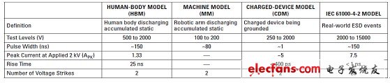
Table 2 Device Level Model vs. IEC System Level Model 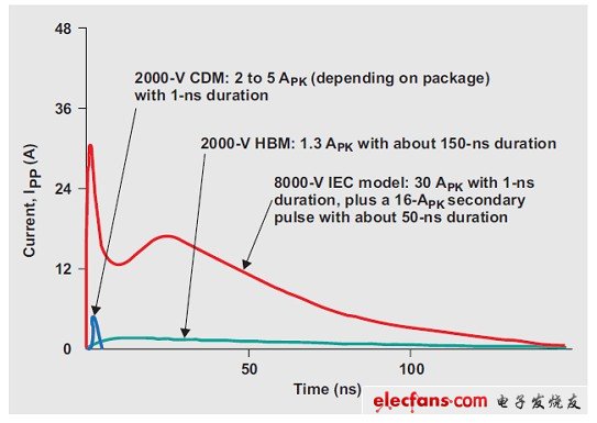
Figure 1 ESD waveforms for device level and IEC models
How TVS protects the system from ESD events
Unlike the ESD protection integrated architecture, the models specified in the IEC 61000-4-2 standard typically use discrete independent transient voltage suppression diodes, also known as transient voltage suppressors (TVS). Independent TVS is less expensive and can be placed close to the system I/O connector, as shown in Figure 2, compared to power management or integrated ESD protection in the microcontroller unit.
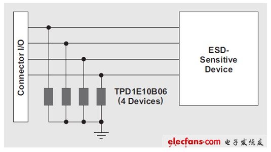
Figure 2 System level TVS layout
There are two types of TVS: two-way and one-way (see Figure 3). The TI TPD1E10B06 is a two-way TVS example that can be placed on a common data line for system level ESD protection. In normal operation, both the bidirectional and unidirectional TVS are open and grounded when an ESD event occurs. In the case of bidirectional TVS, as long as D1 and D2 do not enter their breakdown area, the I/O line voltage signal will swing up and down at the ground voltage. When an ESD shock (positive or negative) hits an I/O line, one diode becomes forward biased and the other breaks down, forming a path through which ESD energy is immediately grounded. In the case of unidirectional TVS, as long as D2 and Z1 do not enter their breakdown region, the voltage signal will swing above the ground voltage. When a positive ESD strike hits the I/O line, D1 becomes forward biased, and Z1 enters its breakdown region before D2; a ground path is formed through D1 and Z1, allowing ESD energy to be dissipated. When a negative ESD event occurs, D2 becomes forward biased and ESD energy is dissipated through the D2 ground path. Since D1 and D2 can be smaller in size and have less parasitic capacitance, unidirectional diodes can be used in many high speed applications; D1 and D2 can “hide†larger Zener diodes Z1 (large size is due to more breakdown areas) Current).
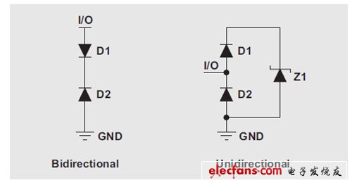
Figure 3 Two-way and one-way TVS
12V 200AH LiFePO4 Battery Pack
Shenzhen Jiesai Electric Co.,Ltd , https://www.gootuenergy.com