For more than a century, almost all technological advances have relied on our ability to produce and manipulate the vast amounts of materials that nature has endowed. This dependence can be seen everywhere, especially in the electronics field. With a wide variety of semiconductors, polymers, and metals, we have been able to create dizzying arrays of circuits that support almost every aspect of modern life.
Now imagine what we can do if we are not limited to the use of materials found in nature. For a long time, researchers have been convinced that one day they may produce man-made materials, or "hypermaterials," and think they will bring some amazing, non-real-world technologies - those that have been in science fiction for years In the technology. These innovations include: invisibility cloaks that mask the presence of objects or their electromagnetic signatures; “non-sensible cloaks†that can mechanically mask the tactile sensation of objects; super lenses that can distinguish small features that ordinary microscopes cannot see; and absorb energy The device can basically capture all the sunlight that shines on the solar cell.
To achieve these advancements, we will need better metamaterials, and they will soon be available. Metamaterials consist of "elementary atoms," which are small, two- or three-dimensional structures made of polymers, dielectric materials, or metals. When these structures exhibit a regular, repetitive array of crystals, they can be used to manipulate electromagnetic radiation in a completely new way. The function of metamaterials ultimately depends on the size, shape and quality of these structures. The technology for manufacturing metamaterials has recently entered a new phase.
Over the past few years, research groups around the world have successfully developed a way to use lasers to draw metamaterials. The resulting structure can now assume almost any shape and accumulates in a dense, crystal-like arrangement in a three-dimensional space. What's more, they can be made into small enough shapes to exhibit unique mechanical and thermal properties, as well as to change the optical flow over a range of wavelengths - including long-term inaccessible visible spectral blocks. Thanks to this micro-manufacturing technology, we can finally see paths beyond the materials that nature has provided us, leading to entirely new areas that are limited only by our imagination.

Despite the richness and variety of natural materials, they actually have some fairly narrow features. This fact is particularly evident in the way materials react to light.
Ordinary atoms (such as silicon and copper) are filled with charged particles and usually interact with the electric field quite strongly. However, electromagnetic waves are composed of two parts: an oscillating electric field and an oscillating magnetic field. The response of a material to a magnetic field is another matter.
Because of some of the quantum mechanics that we will not discuss in depth here, many atoms do respond to the magnetic component of electromagnetic radiation (for example, this reaction makes magnetic resonance imaging possible). However, when the frequency of incident radiation is higher than about 100 GHz—the high-frequency edge value of the microwave portion of the spectrum, most atoms stop resonating the magnetic component of the light and stop responding. This means that, in fact, traditional materials only respond to the electrical components of electromagnetic waves, especially at infrared and visible wavelengths.
This may have ended the study. But in 1999, John Pendry, a physicist at the Imperial College in London, England, and his colleagues pointed out that it should be possible to create transparent structures that can manipulate the electromagnetic components of light at the same time.
To do this, the team designed a metal ring and cut a seam in the side. Like any metal ring, this cracked ring produces an inductance called "L" to resist changes in the external magnetic field. However, because there is a gap in the metal ring, charges will accumulate on both sides of the gap, allowing the metal ring to have capacitance, or "C". The result is an LC circuit. For incident electromagnetic waves of the correct frequency, the split ring will react with an oscillating current and form its own oscillating magnetic field. The smaller the metal ring, the shorter the wavelength at which it reacts.
Penderry and his collaborators made the following inference: By arranging many such artificial materials in a dense, periodic array (a two-dimensional or three-dimensional crystal) it should be possible to create a metamaterial that cannot be made of natural materials. The way it is done responds to incident electromagnetic radiation. In 2000, the team led by David Smith and Sheldon Schultz from the University of California, San Diego conducted the first experiment that truly demonstrated the power of metamaterials.
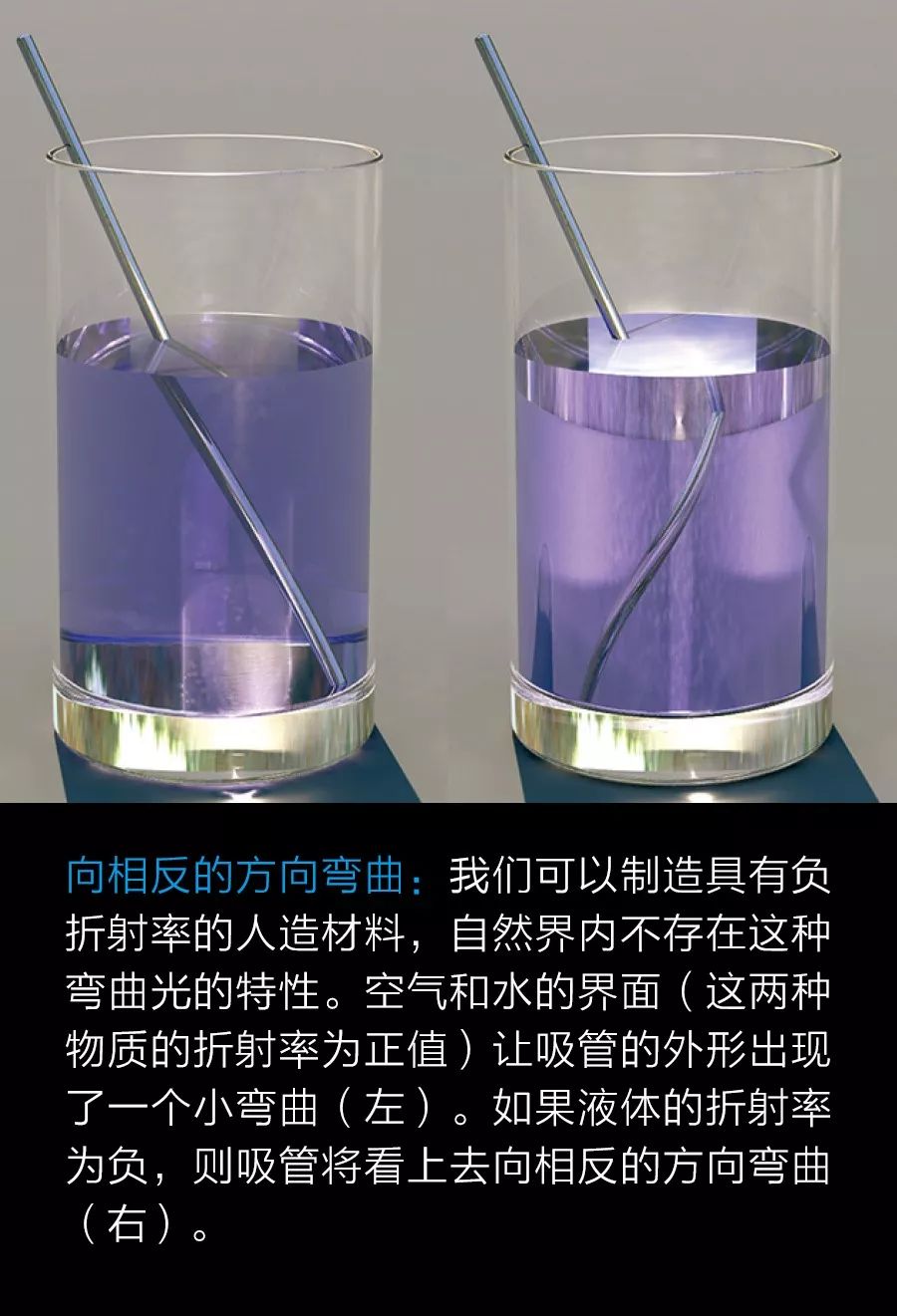
Smith and Schulz built several pairs of 6.5 mm wide, open-ring copper resonators, each separated by about 8 mm, and placed a short wire between each pair of resonators. When the researchers irradiated microwave radiation into this structure, the results showed that the material exhibited an incredible characteristic that did not exist in nature: the negative refractive index.
Materials with this characteristic are more or less "putting light into reverse." To understand how this phenomenon occurs, the best way is to observe two parameters that describe light propagation—the speed and phase velocity of electromagnetic energy. The first parameter describes the total light flow, and the second parameter describes how the individual peaks and troughs of light waves move. In ordinary materials, electrons react to the incident field by vibrating to form their own electromagnetic field. The resulting field, the combination of the incident field and the material reaction, will move in the same direction as the incident radiation, but with a certain lag and a slower speed. For the incident field, the energy and phase vectors are positive. However, in a material with a negative refractive index, energy and phase move in opposite directions. Although the energy of the light and the light itself still move in the direction of the incoming material, the individual crests and troughs actually move backwards.
To describe this phenomenon in the real world, imagine a straw in a half-full glass. If the pipette stands in the water, it looks like it is in the air, but there is a slight kinking at the interface between the two substances. However, if the refractive index of the liquid in the glass is negative, the straw will appear to be curved, as if tilted in the opposite direction.
A material with a negative refractive index may be used to make a super lens, which can image an object with a resolution much lower than the wavelength of the incident light. But the ability to control both components of light at the same time can also provide other possibilities. The elemental atoms that act simultaneously on the electromagnetic component of the radiation can be used to create an "invisibility cloak," acting on the naked eye to divert the light, thereby making the object "invisible."
We may also create a metamaterial that has an electromagnetic response that can undergo destructive interference and therefore does not reflect any radiation. If we can do this in a system that absorbs light, then we can create a completely black material that neither reflects light nor transmits light, increasing the possibility of making more sensitive detectors and more efficient solar cells .
Another possible application is filtering light through left/right circular polarization. The basic mechanism is similar to the way that sugar water, DNA, and other chiral materials - molecules with independent mirror images - rotate the polarization of light waves. In these materials, the interaction is rather weak, requiring the light to travel several centimeters within the material before a strong polarization change occurs. The metamaterial structure is an array of tiny spirals that can perform their filtering tasks at a shorter distance. This may allow us to build a compact device that can distinguish between drugs and their mirror images, both of which may have the same composition but very different biological effects.
â”â”â”â”â”â”
This is only a small part of the potential use of metamaterials. In order to turn the blueprint into reality, we must find a good way to make the underlying structure - the meta-atom.
More than a decade ago, when the metamaterials field was just starting up, the meta-atoms tended to be at the macroscopic level: a 1 cm-sized metal split ring wire on a standard circuit board. But these structures are so large that they may only act on longer-wavelength radiation—in the microwave portion of the spectrum. To make metamaterials that can act on visible light (in the wavelength range of about 400 to 750 nm), the size of the "atoms" must be between 100 and 200 nanometers, or even less.
How to make such a small structure? You may think that naturally you should first use the technology that has been developed in the semiconductor industry. After all, there are already some very powerful graphical tools, such as photolithography and electron beam lithography, that are commonly used to fabricate submicron and nanostructures.
In fact, many research groups - including Harald Giessen of Stuttgart University in Germany, Vladimir Shalaev of Purdue University in Indiana, USA, and Iowa State University Costas M. Soukoulis, Xiang Zhang of the University of California, Berkeley, Nikolay Zheludev of the University of Southampton, UK, and us in Kars, Germany The Research Group at the Ruhe Institute of Technology (KIT) has successfully used these technologies to create simple metamaterial structures, including open-loop resonators, small enough to act on visible or infrared light.
However, when you try to create even seemingly simple 3D objects, these lithography methods begin to fail. At this point you need metamaterials that can act on light in any direction. Photolithography is intended to create patterns with 2D properties, so if you are building an array of tiny spiral coils, you must build it layer by layer in hundreds of steps. This is a very time-consuming process that requires careful adjustment. Even a research team who is skilled in this process may need a full day to build a single layer.
Fortunately, we have a better way to build a 3D structure. The key is to use lasers and some techniques developed in the past few years to write in three-dimensional space. You can consider this type of optical lithography, direct laser writing, as a microscopic version of 3D printing. Just like rapid prototyping, or stereolithography, which Charles W. Hull obtained in 1986, light is used to outline shapes. However, in this case, the shape is not made layer by layer. Instead, they are formed using a single volume of material. The solvent washed away parts that were not exposed to light, just as Michelangelo described the artist's creation of a statue: knocking out excess stones little by little.
â”â”â”â”â”â”
As with other lithography techniques, laser direct writing uses a compound called a resist—in this case, a photosensitive mixture called a photoresist. To make metamaterials, we start with a thicker layer of objects, wrapped in glass slides or some other substrate, and mounted on a microscope. When we let the laser pass through the optical microscope and hit the photoresist, the light breaks the molecular structure, causing the exposed material to polymerize and solidify. After completion, we can use solvents to wash away unexposed material leaving only the exposed material.
Normally, this method only produces good results in two dimensions. This is because even if we focus the laser on the inside of the resist, not only the photons near the focal region are absorbed, but also the photons (including the top and bottom of the focal point) in the entire beam cone are absorbed. In order to allow the curing process to work properly in three-dimensional space, we have slightly changed our strategy to match the "photoinitiator" - the part of the photoresist that absorbs photons - with a longer wavelength laser. If the combination of the two is just right, we can create a system where photoinitiators must absorb two photons (rather than one) to be excited.
If two photons are needed, the absorption response is not linear; instead, it is proportional to the square of the light intensity. If we double it, we get four times the response. This helps to limit the effect of the laser: If the laser beam is tightly focused, the exposure will be limited to a small part around the focal point. Then, to draw any 3D shape, we simply move the focus around by moving the sample or laser beam.
However, this technique may not necessarily allow us to obtain sufficiently small elementary atoms to interact with light. The limitations imposed on this are the Abbe diffraction barrier, a characteristic of the microscope optics that limits the spatial resolution of the lens, thereby limiting how closely you can put two adjacent features or rays together. For 800 nm lasers (which can use ordinary photoresists) and high-end microscope lenses, you will be limited to a lateral distance of around 300 nm due to the Abbe diffraction barrier.
For decades, the Abbe diffraction barrier seems to have become the basic limit. But about a few years ago, we proved that there was a way to break it. The physicist Stefan Hell first proposed this idea. He is currently working at the Max Planck Institute for Biophysical Chemistry in Göttingen, Germany. In the early 1990s, he proposed a method to break the diffraction barrier by using a second laser that operates at different frequencies.
Through a process called "stimulated emission loss," the second laser can cause an excited molecule to "spit" a photon and relax back to a lower energy state. This is very useful for photolithography, because it actually gives us an "eraser" that matches the "pen" used. The write beam will generate a hot spot in the center, and the erase beam will have a different cross-section: a special shape focus with zero intensity, at the position where the write laser is at the maximum (see the figure "Write through the resist" "). When using two beams, everything outside the true center of the writing beam is desensitized and the photoresist there remains unexposed.

The interest of the Hale group is that using this technique causes the stained cells and other biological structures to glow in as tiny a spot as possible, so that they can be imaged with very high resolution under the microscope. (His team has made great progress in this area: in 2009, they discovered that visible light can be used to analyze features under a microscope with an accuracy as small as 6 nanometers. This range can only pass through a few atoms and is much lower than the Abbe diffraction barrier. .)
However, it is not easy to use a double laser beam method to cure the photoresist. We started to study this possibility in 2008 at the KIT group, and there was no photoresist specifically developed to support this method. One of the problems we encountered early on was that the design of photoinitiators was very efficient; after being hit by photons, they reacted almost instantaneously, so fast that the second laser beam could not deextend molecules and stop the polymerization reaction. We spent a year conducting research. We made some trials and made some mistakes. However, we finally found a photoinitiator (a dye molecule that was only used prudently in photolithography at that time) to achieve an effect. .
With this photoinitiator, we found that the structure can be printed with a lateral resolution of approximately 175 nm (the distance between two adjacent features), which is approximately 40% higher than the resolution that can be achieved under the Abbe limit. .
This is a considerable improvement. However, in principle, using 800 nm of light should be possible with a spatial resolution of several tens of nanometers (exceeding the resolution at which you start to reach the molecular scale). Reducing the resolution of this lithography to this scale will require more work. The problem is no longer optical components, but the photoinitiators we use. Due to some of the reasons that are still being explored - perhaps the diffusion of photoinitiator molecules themselves, attempts to make smaller structures often result in ill-defined features. For example, if you try to make two features that are less than 175 nm apart, you may end up curing areas that should not be part of the final shape.
Despite this, the current resolution is enough to allow us to create artificial materials that can work in the visible part of the spectrum. Many of these materials were not even made at all until a few years ago.
Back to our favorite example of discussion - the invisibility cloak: When we started to study this issue in early 2009, other groups have succeeded in creating structures that can hide objects in two dimensions. But if you want to accomplish this feat in light wavelengths and three-dimensional space, you need more planning.
In terms of design guidelines, we rely on the work done by metamaterial theorists, such as Pendry at Imperial College and Ulf Leonhardt of St. Andrews University in Scotland, who showed how The attributes you wish to have have reverse engineered the metamaterial design. The trick is to use coordinate transformations that are somewhat similar to the coordinate transformations in Einstein's general relativity that are used to calculate how quality distort the spatio-temporal structure. These allow you to derive the structure of the metamaterial in the way you wish to influence the flow of light.
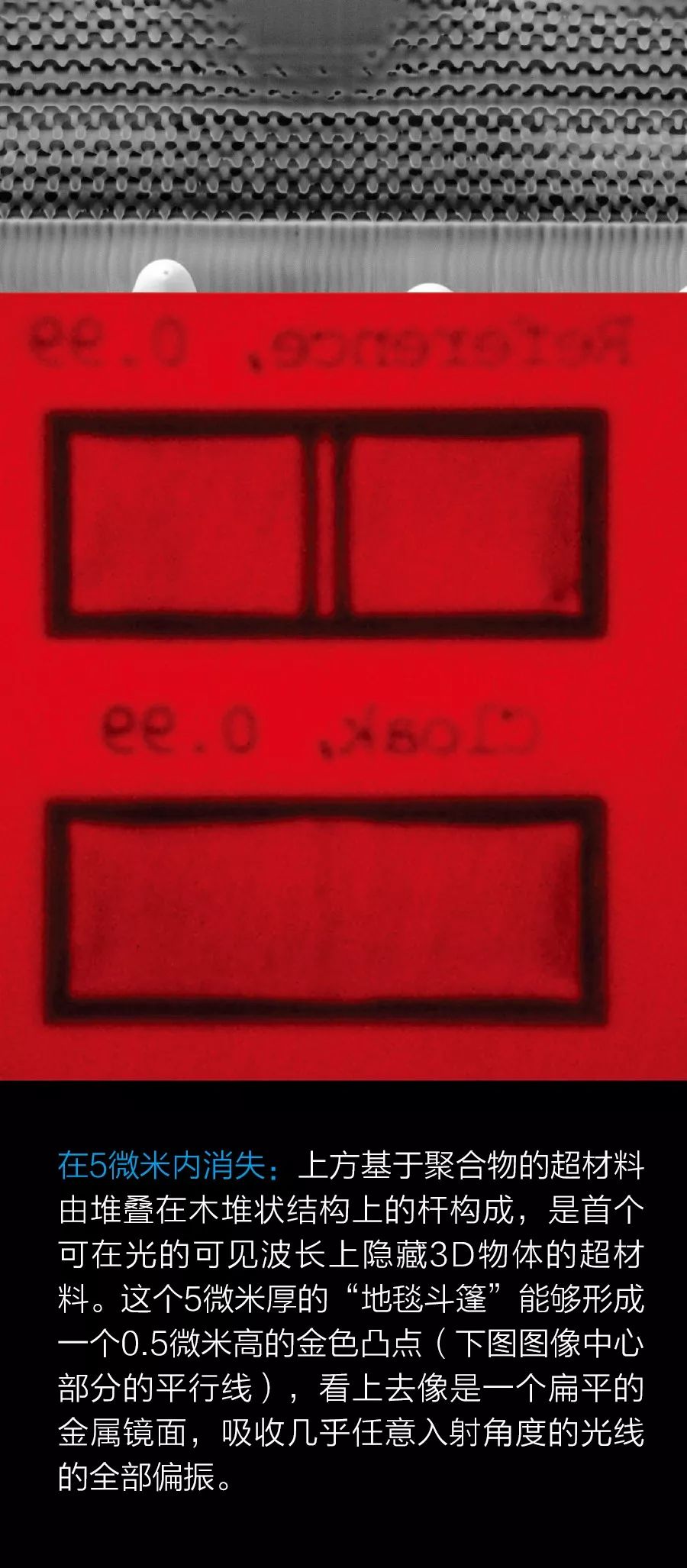
Due to the use of laser direct writing, invisible cloaks that can operate at visible wavelengths have become a reality. We have not used them to hide objects that are as large as the human body. But we used them to change the appearance of some smaller objects. The 3D "carpet cloak" we built (see illustration "disappears within 5 microns") is based on a restricted geometry, but does apply to visible light, and across a wide range of frequencies, it allows a curved floor (carpet ) It looks like a flat metal mirror.
The metamaterials series now includes many creations that previously seemed impossible. Some recent inventions include titanium dioxide-based photonic crystals that are capable of completely reflecting visible light from any direction and can be used to direct the light emitted by the LED. Five-mode mechanical metamaterials (liquid-like solids) are also available. These can be used to make "non-sensible cloaks," so that the presence of objects cannot be detected by touch. We have also succeeded in creating 3D photonic quasicrystals, optical counterparts to Dan Shechtman's 2011 physical structure of the Nobel Prize in Chemistry. Although we are still exploring the application of this special material, laser direct writing is the only way to make complex underlying structures.
â”â”â”â”â”â”
In all of this exciting manufacturing work, one innovation has dramatically changed the manufacturing process. Early laser writing was limited by microscope optics: the slides had to be placed between the objective and the photoresist of the microscope. This arrangement means that the thickness of the metamaterial does not exceed about 100 microns.
However, in 2012, Nanoscribe (a company developed from studies completed in our laboratory) proposed a new method to solve this problem. In an immersed microscope, the objective lens of the microscope is coated with oil droplets between the lens and the glass slide. Nanoscribe created a special photoresist that emits just enough to replace the oil droplets, allowing the resist to drop directly onto the lens.
Without this two-photon absorption, this solution certainly would not be a good idea. The photons from the lens solidify the photoresist on the beamline, causing the latter to stick to the lens and destroy the lens after the first use. Two-photon absorption allows us to locate the curing process in three dimensions.
This "immersed" approach also allows us to build structures on surfaces other than glass. And since the resist and lens are no longer separated by a thick glass substrate, we can extend the focus by about 10 times so that we can enter the sample and create a 3D metamaterial array with a height of 1 mm. This is close to the height at which we begin to consider the construction of macro metamaterials - objects that are large enough to hold in their hands, not just thin, fragile coatings.
Of course, there is still room for improvement. The resolution of laser writing is barely enough to make a metamaterial that can manipulate light that can operate at visible light frequencies. Some of the more complex structures, such as metal spiral forests, still cannot be manufactured and will most likely require entirely new photoresists. But at least in principle, no obvious factors will lead to failure.
We must also solve the problem of writing speed. In this regard, we have actually made good progress. In the research lab, we fixed the laser and used a high-precision 3D piezoelectric actuator to move the sample to draw the structure. In general, the speed of these jobs is about 100 microns per second. For many structures, it takes about half an hour to create a metamaterial with a footprint of 100 microns by 100 microns. But recently, Nanoscribe and other companies have adopted a laser scanning system based on a 2D galvanometer, which allows faster writing speeds up to 1 meter per second. Using these commercially available lithography tools, we can increase manufacturing speed by a factor of 100.
Metamaterials are just the beginning. With the recent speed improvement and further improvements in spatial resolution, we believe that laser direct writing may counterbalance planar electron beam lithography in the future. The latter is currently used to fabricate masks for stencils, to identify logic and circuits on memory chips. layout.
Of course, there are more. By transforming active elements such as nanodiamonds into emitting a single photon, we can even conceive of creating a three-dimensional optical system for chip-based quantum information processing.
We are just beginning to explore the application of these new manufacturing tools. But in the future, the structure of matter may become infinitely complex and sophisticated.
This PS5 docking station have several design, some come with AC adapter with UL certificates, some soem with Type-C adapter,all docking are hiqg quality with CE FCC RoHS.
Features:
Charge two (2) PS5 DualSense Controllers simultaneously.
Built-in intelligent IC protection provides overheat, overcharge, overcurrent, and short circuit protections so you can charge your PS5 DualSense Controller with a total peace of mind.
Can be powered the USB port from either the PS5 console or AC adapter
Lightweight and compact design for easy placement.
USB-C dongle for place and charge function, which is easy to be inserted in or pulled out from charger station.
Low standby power consumption, power-saving and environmental protection.
- [Fast Charging]5V/2A input fast Type-C charging ports for two PS5 DualSense controllers simultaneously. Please note: Only if the input power source is at least 5V/2A, the controllers can be fully charged under 4 hours.
- [Onboard Chip Protection]Charging station comes with the built-in protector chip, which provides over-charge,over-voltage, over-temperature, short-circuit protection.
-
[LED Charging Display]When charging , it has LED indicator to show the charging status.


Ps5 Charging Dock,Ps5 Charging Dock Station,Portable Ps5 Charging Station,Ps5 Charging Dock Stand
Shenzhen GEME electronics Co,.Ltd , https://www.gemesz.com